Hi to everyone !
i'm back to experimentation...
I've just turned a pc smps into a chip amp (TDA7294) power supply in the 200-300W range.
no change in primary side (classical pc smps)
half bridge topology
voltage mode regulation with PWM chip TL494
MJE13009 bipolar switches
xformer proportional base drive
36 mm toroid main transformer from a car amplifier smps
fsw=31 khz
240VAC 50Hz input
unregulated it provides +/-39V with no load +/- 34V @250W
regulated it gives +/-30V
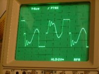
question : is it a normal waveform for the secondary voltage ?
here are pics:
i'm back to experimentation...
I've just turned a pc smps into a chip amp (TDA7294) power supply in the 200-300W range.
no change in primary side (classical pc smps)
half bridge topology
voltage mode regulation with PWM chip TL494
MJE13009 bipolar switches
xformer proportional base drive
36 mm toroid main transformer from a car amplifier smps
fsw=31 khz
240VAC 50Hz input
unregulated it provides +/-39V with no load +/- 34V @250W
regulated it gives +/-30V
question : is it a normal waveform for the secondary voltage ?
here are pics:
Attachments
Hi alexclaire,
Interesting project.
I don't know if that waveform is 'normal' or not. It looks pretty good, to me, not knowing exatly where it came from.
If you post a schematic, maybe someone can tell you the answer to that question.
But it does look like an RC snubber network might be a good idea, to try to eliminate the high-frequency ringing. Again, a schematic would help a lot, to decide where it should be placed, etc.
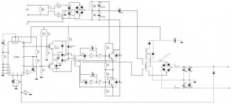
here is the schematics.
overload protection on primary side not yet implemented (current sense transformer)
I'd like to know if the secondary voltage waveform is normal
(red line on schematics)
this smps gives +/-30V and supplies a 7294 chip amp with no problem
no noise at output...
duty cycle increases as the output of amp becomes louder (normal behaviour) but there is a kind of sinusoide on this square wave...
regulation loop ?
need some tips about voltage regulation...
thanks for reply !
Attachments
some measurements :
output +/- 29v regulated
when amp pushed to clipping (~27v peak) = 45W rms @8ohms
i can hear strange noise from smps (hiss in power transformer ?)
when this smps runs in open loop (no voltage regulation)
output voltage with no load +/- 39V
output voltage @250W +/- 35V
no strange noise at all
so the noise comes from this bad voltage regulation ?
need some kind of compensation in this feedback loop ?
need some help to understand this mode of regulation
thanks !
The shown (o-scope) waveform at the output doesn't look very healthy  .
.
More interesting would be the waveform across C23 or between pin 12 of the TL494 to GND (i.e. pin 7, 9, ...), to make sure the power supply for the TL494 is OK.
Basically, many SMPS I've repaired using a TL494 as PWM controller have their own power supply which was derived by a separate and standard auxiliary mains (50/60Hz) transformer. Your schematic shows a power supply derived from a secondary winding of the power transformer. A start-up winding is supplied on the driving transformer TR1 (if I deciphered the reference on the schematic correctly).
Once in a while I've experienced trouble with this configuration when rapidly and strongly changing load conditions occure.
There're good reasons for using a 3-terminal (linear) regulator (i.e. 7815) to power the TL494.
For further investigations I would like to see the signal of both collector potentials at the driver trannies (T4 & ..: 2SC945(?)). Besides - have you checked the two diodes connected in series going from the two driver trannies (emmitter) to GND? And how about the 1µF capacitor, C6(?), in parallel to them? No short? I've often found this particular capacitor shorted and the diodes, or at least one of them, blown making an open circuit.
.More interesting would be the waveform across C23 or between pin 12 of the TL494 to GND (i.e. pin 7, 9, ...), to make sure the power supply for the TL494 is OK.
Basically, many SMPS I've repaired using a TL494 as PWM controller have their own power supply which was derived by a separate and standard auxiliary mains (50/60Hz) transformer. Your schematic shows a power supply derived from a secondary winding of the power transformer. A start-up winding is supplied on the driving transformer TR1 (if I deciphered the reference on the schematic correctly).
Once in a while I've experienced trouble with this configuration when rapidly and strongly changing load conditions occure.
There're good reasons for using a 3-terminal (linear) regulator (i.e. 7815) to power the TL494.
For further investigations I would like to see the signal of both collector potentials at the driver trannies (T4 & ..: 2SC945(?)). Besides - have you checked the two diodes connected in series going from the two driver trannies (emmitter) to GND? And how about the 1µF capacitor, C6(?), in parallel to them? No short? I've often found this particular capacitor shorted and the diodes, or at least one of them, blown making an open circuit.
The 'auxiliary' winding on the driver xfmr is the Proportional-Base Drive Alex mentioned. Basically, the primary side is a free-running oscillator for the first few cycles at start-up. When voltage sufficient to power the '494 is generated across the secondaries, the PWM chip takes over control. The '494 doesn't actually "drive" the switches, but merely controls their turn-off time, since its RC time-constant is shorter than the oscillator's time-constant. This setup eliminates the need for a separate, dedicated power supply for the '494.
For a great detailed explanation on how proportional-base drive works, look at the Nov 04 issue of QST. Phil, KF6ZZ, does a great job describing it in his article on modding an AT/ATX smps for +13.8V-only, for powering radios & other 12V stuff.
Steve
For a great detailed explanation on how proportional-base drive works, look at the Nov 04 issue of QST. Phil, KF6ZZ, does a great job describing it in his article on modding an AT/ATX smps for +13.8V-only, for powering radios & other 12V stuff.
Steve
@Steve: I'm sorry that I was misunderstood - maybe it's because I didn't choose the right words and/or phrases. I'm aware of the circumstance that at start-up a self-oscillation is necessary. I just wanted to point at the path (not exactly at the winding - so again, sorry for that) that is necessary for any self-oscillation.
Besides that, I'm sure there's a reason why so many manufacturers are using a standard mains transformer (3...4 watt) to supply the TL494 in the same SMPS topology. I can imagine that it might be an issue with complexity, production costs, etc.
I'm not so deeply involved in designing PC-SMPS, I've just repaired and modified (even misused/abused") ) numerous of them for my own purposes.
) numerous of them for my own purposes.
@Alex:
But back to the issue you've reported:
If both driver and both power trannies are working, I must say that, according to your o-scope screenshot which I just compared to a perfectly working design on my bench, your sinusoidals amplitude is much to high. I measured just 1/5 to 1/6 of the amplitude of the square wave part. And that could be a result of a to high leakage inductance!
I guess you've unwound/rewound the secondary or just added a bunch of windings in order to get the higher output voltages for the TDA7294. To lower the leakage inductance you might have to reorder/rearrange/rewind the power transformer.
So please Alex, give us a hint on how you've arranged the additional windings on you power transformer.
Besides that, I'm sure there's a reason why so many manufacturers are using a standard mains transformer (3...4 watt) to supply the TL494 in the same SMPS topology. I can imagine that it might be an issue with complexity, production costs, etc.
I'm not so deeply involved in designing PC-SMPS, I've just repaired and modified (even misused/abused
) numerous of them for my own purposes.@Alex:
But back to the issue you've reported:
If both driver and both power trannies are working, I must say that, according to your o-scope screenshot which I just compared to a perfectly working design on my bench, your sinusoidals amplitude is much to high. I measured just 1/5 to 1/6 of the amplitude of the square wave part. And that could be a result of a to high leakage inductance!
I guess you've unwound/rewound the secondary or just added a bunch of windings in order to get the higher output voltages for the TDA7294. To lower the leakage inductance you might have to reorder/rearrange/rewind the power transformer.
So please Alex, give us a hint on how you've arranged the additional windings on you power transformer.
Hi corax !
thanks for your reply
some precisions about my main transformer:
it's a toroid of unknow material (suitable for power application: it's from a car amplifier smps ) diam.36mm
primary : 40 turns unifilar diam.0.6mm
aux secondary : 2 X 5 turns unifilar 0.6mm
main secondary : 2 X 10 turns bifilar 0.6mm wound on the hole core
Cross section area is about 1 cm2
at idle the temperatue of the core rises a little because of Bmax of 330mT (3300 Gauss)
without feedback : secondary voltage before rectifier is a perfect square wave (0V---40V) even loaded @ 250W (just dead time appears)
with feedback : secondary voltage before rectifier is the pic i gave before...
- Status
- This old topic is closed. If you want to reopen this topic, contact a moderator using the "Report Post" button.
- Home
- Amplifiers
- Power Supplies
- half bridge smps for chip amp voltage regulation question