Hello everyone!
I'm currently working on a flyback converter, and I need a little advice. Sorry in advance for the long post...
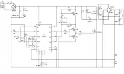
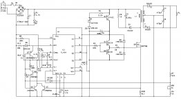
The converter is based on the TL494, and is ~34-40V DC input, +/- 18V @ 3A output. I meant it to be a scaled-down version of an offline converter I will be designing later, so I can get some practice with the topology, and so that I can use up an old 27VAC, 150VA transformer. My target efficiency is a modest 80%, but I will get to that later. Unfortunately, I will be driving an existing class AB amp, so my load will range from around 100mA quiescent to up to 3A. I've designed the converter with the 3A upper limit as my design point, but this does not seem to be working out efficiency-wise. The schematic I've attached is a scaled-down version of the final supply, with most of the features removed for testing.
Right now, the supply is working and producing the correct, regulated voltages. I realize the bridge in the secondary is odd, but as far as I can tell it should work (unless I've missed something fundamental here). The gate drive waveforms look clean (will post pictures later) - the external transistors are there since I plan to use multiple mosfets with this design later.
My problem(s) are as follows:
* When loaded from around 100mA-500mA, the supply hovers around 50% efficiency, as best I can measure. I expected this to be the case. With a 1A load (my current maximum), efficiency rises to 60%. Can I expect to achieve my maximum efficiency at full load only (3A)? If so, I suspect I will be wasting lots of energy at normal listening levels. I also think that this may be a bit lower than the final product, since I have only prototyped it on a breadboard, so I^2R and parasitic losses are high. I have calculated the transformer windings for a load of 3A nominal - was this incorrect? I have verified that my windings produce the expected inductance by measuring the final transformer.
* More about the transformer - I think my loses may be coming from here. The core is a rescued E-I core from a computer PS, which I unfortunately cracked. I have compensated for the additional air gap by adding more windings (and measuring the value so it is the same as designed). Is this air gap causing me additional problems that I am not aware of?
* I have one final problem, which is the most worrying. During testing, I used a set of old FR103 diodes (1A, fast recovery) for the output bridge. This worked fine for the small loads. However, in anticipation of full-load testing, I changed to the final FR603 (6A, same series) diodes. Immediately after this, the supply began emitting a (very loud) audible screeching noise on the 1A (36 ohm resistor) load. I was not brave enough to leave it on for long, but I did verify that the input current and output voltage were almost unchanged. There now appears to be serious ringing on the mosfet drain, to the point where audible noise is produced. I have increased dissipation in the snubber to compensate (the values you see there are from testing, and are far from those I calculated from the leakage inductance). However, nothing seems to tame the voltage spikes
very much - I am not sure if I should continue testing (the noise is *very* loud), especially with higher loads. Any ideas on how I should proceed here? More snubber modifications? Rewind the core? Or just toss on a 2A/3A load and see what happens?
My original design also has pulse-by-pulse current limiting and under-voltage lock-out, but I will tackle these after the basics. Sorry again for the long-winded post, but I really want to finish this one")
I'm currently working on a flyback converter, and I need a little advice. Sorry in advance for the long post...
The converter is based on the TL494, and is ~34-40V DC input, +/- 18V @ 3A output. I meant it to be a scaled-down version of an offline converter I will be designing later, so I can get some practice with the topology, and so that I can use up an old 27VAC, 150VA transformer. My target efficiency is a modest 80%, but I will get to that later. Unfortunately, I will be driving an existing class AB amp, so my load will range from around 100mA quiescent to up to 3A. I've designed the converter with the 3A upper limit as my design point, but this does not seem to be working out efficiency-wise. The schematic I've attached is a scaled-down version of the final supply, with most of the features removed for testing.
Right now, the supply is working and producing the correct, regulated voltages. I realize the bridge in the secondary is odd, but as far as I can tell it should work (unless I've missed something fundamental here). The gate drive waveforms look clean (will post pictures later) - the external transistors are there since I plan to use multiple mosfets with this design later.
My problem(s) are as follows:
* When loaded from around 100mA-500mA, the supply hovers around 50% efficiency, as best I can measure. I expected this to be the case. With a 1A load (my current maximum), efficiency rises to 60%. Can I expect to achieve my maximum efficiency at full load only (3A)? If so, I suspect I will be wasting lots of energy at normal listening levels. I also think that this may be a bit lower than the final product, since I have only prototyped it on a breadboard, so I^2R and parasitic losses are high. I have calculated the transformer windings for a load of 3A nominal - was this incorrect? I have verified that my windings produce the expected inductance by measuring the final transformer.
* More about the transformer - I think my loses may be coming from here. The core is a rescued E-I core from a computer PS, which I unfortunately cracked. I have compensated for the additional air gap by adding more windings (and measuring the value so it is the same as designed). Is this air gap causing me additional problems that I am not aware of?
* I have one final problem, which is the most worrying. During testing, I used a set of old FR103 diodes (1A, fast recovery) for the output bridge. This worked fine for the small loads. However, in anticipation of full-load testing, I changed to the final FR603 (6A, same series) diodes. Immediately after this, the supply began emitting a (very loud) audible screeching noise on the 1A (36 ohm resistor) load. I was not brave enough to leave it on for long, but I did verify that the input current and output voltage were almost unchanged. There now appears to be serious ringing on the mosfet drain, to the point where audible noise is produced. I have increased dissipation in the snubber to compensate (the values you see there are from testing, and are far from those I calculated from the leakage inductance). However, nothing seems to tame the voltage spikes
very much - I am not sure if I should continue testing (the noise is *very* loud), especially with higher loads. Any ideas on how I should proceed here? More snubber modifications? Rewind the core? Or just toss on a 2A/3A load and see what happens?
My original design also has pulse-by-pulse current limiting and under-voltage lock-out, but I will tackle these after the basics. Sorry again for the long-winded post, but I really want to finish this one
Attachments
Hi,
You can simplify the voltage regulator to the MOSFET gate drive buffers since the net current draw of those bipolar emitter followers is very low.
I think a lot of the noise you hear is loop instability. Some topologies are more prone to this problem. Its been a while since I have worked with flyback and forward circuits for anything more than flea power levels, so I anticipate more specific suggestions from people.
- Your secondary side rectification arrangement is not valid for a flyback. See other flyback schematics (or flyback basics on wikipedia http://en.wikipedia.org/wiki/Flyback_converter ). Secondary windings have to be half wave rectified in such a way that the diode does not conduct when the primary side MOSFET is ON.
- A flyback without cycle by cycle peak current limiting is very prone to self destruction. Overcurrent coditions are narutally triggered at power up and during any big load transient. TL494 does not allow for peak current limiting without a lot of additional components, so you should consider more suitable ICs like UC3842.
- You should consider regulating the voltage that powers the complete control IC rather than limiting the output voltage of the gate drive buffer. Your arrangement causes reverse biasing of Q1 and huge dissipation in R3 at high input voltages.
- A gapped tansformer with low leakage inductance, known magnetizing inductance and known saturation current is required for a flyback. You seem to be using the core without any gap. I have published a circuit that allows easy measurement of transformer and inductor parameters with the help of an oscilloscope: http://www.diyaudio.com/forums/showthread.php?s=&threadid=77919&highlight=
- A flyback requires proper duty cycle limiting (like 70%). You are already achieving a 50% limit with the help of the flip-flop output mode of the TL494 (and frequency is effectively halved), although yours is a really risky arrangement because the outputs are in an high impedance state during most of the time and the MOSFET can easily turn itself on and off due to parasitistics. You should use a normal parallel arrangement with active turn-on and buffered turn-off instead.
First, thank you both so much for the replies!
Electrone:
I agree, there is very likely some loop instability at the moment – probably from induced noise and whatnot. I will have to be careful with my final layout to avoid this.
As for the regulator, I will explain in a second – short answer: mistake on the diagram
Eva:
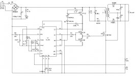
1) I figured as much. I guess I shouldn’t try to “improve” (read: mess with) a design until I have it working first. I’ll be working on your suggestions one at a time, so this first schematic has the proper rectifier set-up shown. Is this correct/acceptable, or should I rewind for completely separate secondaries? (Rather than the center tap arrangement I have now)
2) I’ve already lifted the current limiting from this application note:
http://focus.ti.com/lit/an/slva001d/slva001d.pdf
I agree that it is more complicated, so I will probably use a different chip for my next project. I selected the TL494 for this one since I had at least a little familiarity from making some Buck converters with it. I will add it next, as you suggest.
3) Oops! Pilot error on this one… was tired when re-drawing the schematic. This schematic now shows the actual arrangement, where the entire drive section/IC is powered from the 15V regulated. I realize this is inefficient; it is fine for me in this design as long as the wasted power doesn’t become too great. For my offline design I will use a proper start-up circuit and auxiliary winding for this purpose.
4) I have gapped the transformer and measured its leakage and magnetizing inductance. However, there is a good chance my measurements are flawed – I will definitely be building the project you linked, it looks significantly easier to use. I will tackle the transformer after the other circuit changes.
5) I should be able to achieve duty cycle limiting using the dead-time input on the 494 again (will be quite busy there with the current limiting and soft-start). I understand what you are saying for the gate drive, but I am unsure of the details. I will make the other changes first, and then post my attempt. For simplicity, could I simply use the 494 outputs directly? I am concerned over their rating for use with anything other than a single mosfet, though. I was thinking something like the arrangement shown here (Page 20, upper left arrangement):
http://www.freeradio.org/documents/Switching_Power_Supply.pdf
If not, I will be back for more advice on designing a proper gate drive. For now, though, I will make the rectifier changes and check back with results.
Electrone:
I agree, there is very likely some loop instability at the moment – probably from induced noise and whatnot. I will have to be careful with my final layout to avoid this.
As for the regulator, I will explain in a second – short answer: mistake on the diagram
Eva:
1) I figured as much. I guess I shouldn’t try to “improve” (read: mess with) a design until I have it working first. I’ll be working on your suggestions one at a time, so this first schematic has the proper rectifier set-up shown. Is this correct/acceptable, or should I rewind for completely separate secondaries? (Rather than the center tap arrangement I have now)
2) I’ve already lifted the current limiting from this application note:
http://focus.ti.com/lit/an/slva001d/slva001d.pdf
I agree that it is more complicated, so I will probably use a different chip for my next project. I selected the TL494 for this one since I had at least a little familiarity from making some Buck converters with it. I will add it next, as you suggest.
3) Oops! Pilot error on this one… was tired when re-drawing the schematic. This schematic now shows the actual arrangement, where the entire drive section/IC is powered from the 15V regulated. I realize this is inefficient; it is fine for me in this design as long as the wasted power doesn’t become too great. For my offline design I will use a proper start-up circuit and auxiliary winding for this purpose.
4) I have gapped the transformer and measured its leakage and magnetizing inductance. However, there is a good chance my measurements are flawed – I will definitely be building the project you linked, it looks significantly easier to use. I will tackle the transformer after the other circuit changes.
5) I should be able to achieve duty cycle limiting using the dead-time input on the 494 again (will be quite busy there with the current limiting and soft-start). I understand what you are saying for the gate drive, but I am unsure of the details. I will make the other changes first, and then post my attempt. For simplicity, could I simply use the 494 outputs directly? I am concerned over their rating for use with anything other than a single mosfet, though. I was thinking something like the arrangement shown here (Page 20, upper left arrangement):
http://www.freeradio.org/documents/Switching_Power_Supply.pdf
If not, I will be back for more advice on designing a proper gate drive. For now, though, I will make the rectifier changes and check back with results.
Attachments
 Ahh, OK concerning the diagram correction. Even though I am up to phase shift modulated bridge circuits in terms of level of work in the field, I think you are absolutely doing the right thing beginning at the bottom. You will be able to observe problems and think of corrections to try. Otherwise, there is no motivation to use circuits for which you have no known reason why the extra complexity is useful.
I have to admit, I forget most of the reasons why I have gotten where I am in circuit topology, but I realize that I made each judgment based on the experimental results I was getting at the time of each decision.
Hello again, and thanks for the help!
I agree Electrone, starting with a simple flyback has been a good learning experience so far. I’ve become a bit rusty in power electronics a few years out of undergrad, so I figured it was time to tackle a project I’ve been meaning to do for a while anyway.
Also, thank you both for the help! I have now reached around 70% efficiency with a light to moderate load. I believe most of the problem was the output rectification, as Eva said. I am currently using both secondary windings with a single diode for testing (single, 36V output). The snubber value shown still reflects the values determined from testing, with R8 higher now as Eva suggested. The audible noise is now gone, and the voltage spikes have tamed. Also, the snubber values shown are much closer to those calculated, so I seem to be on the right track.
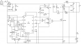
I will now add pulse-by-pulse current limiting, as I mentioned last time. The updated diagram is attached. From simulations, limiting should trigger around 6.5-7A, which is sufficient to save the mosfet from destruction. I plan to test it by triggering the base of Q5 manually, rather than by actually tripping the current limit. Unfortunately, I do not have a Schottky diode handy for D9. I will try the diode with the lowest forward drop I can find, but it may not be able to trigger the reset condition. I am also assuming that 1N4148 diodes should be fine for D7, D8. Please let me know if there are any obvious errors, though I will probably find them during testing tomorrow.
Some stats:
Maximum tested load (this run):
Vin = 38V, Rload = 78.7 ohms, Vout = 37.15V (fixed resistors, nominal = 37V)
Efficiency = 69.4%
I agree Electrone, starting with a simple flyback has been a good learning experience so far. I’ve become a bit rusty in power electronics a few years out of undergrad, so I figured it was time to tackle a project I’ve been meaning to do for a while anyway.
Also, thank you both for the help! I have now reached around 70% efficiency with a light to moderate load. I believe most of the problem was the output rectification, as Eva said. I am currently using both secondary windings with a single diode for testing (single, 36V output). The snubber value shown still reflects the values determined from testing, with R8 higher now as Eva suggested. The audible noise is now gone, and the voltage spikes have tamed. Also, the snubber values shown are much closer to those calculated, so I seem to be on the right track.
I will now add pulse-by-pulse current limiting, as I mentioned last time. The updated diagram is attached. From simulations, limiting should trigger around 6.5-7A, which is sufficient to save the mosfet from destruction. I plan to test it by triggering the base of Q5 manually, rather than by actually tripping the current limit. Unfortunately, I do not have a Schottky diode handy for D9. I will try the diode with the lowest forward drop I can find, but it may not be able to trigger the reset condition. I am also assuming that 1N4148 diodes should be fine for D7, D8. Please let me know if there are any obvious errors, though I will probably find them during testing tomorrow.
Some stats:
Maximum tested load (this run):
Vin = 38V, Rload = 78.7 ohms, Vout = 37.15V (fixed resistors, nominal = 37V)
Efficiency = 69.4%
Attachments
Here is the waveform of the drain voltage (with gate drive too). Sorry for the poor picture quality, I could not find the capture cable for our scope and had to use my camera. Top waveform is gate drive (10V/div), bottom is Vds (10V/div). This is with the final snubber values from above – not too bad.
Attachments

Finally, here is the waveform of the gate drive enlarged. Top is taken from pin 9 on the TL494, and the bottom is Vgs. Both are 10V/div. Note the noise on Vgs after switch-off. As far as I can determine, this is from parasitic capacitance, mostly the capacitve-coupling between the breadboard traces (drain to gate) near the mosfet. Hopefully an improved gate drive will ensure this does not cause false triggering of the mosfet.
t_rise = 270ns, t_fall = 210ns (Vgs)
Next step is to try to track down my remaining losses. I suspect I will hit the wall soon and have to move from the breadboard to a more finished form. I also think that a lot of my remaining losses are in the transformer construction. I will build/test the current limiting tomorrow, and post the results plus the new gate drive design also. Then I can try to wind a better transformer. I will probably be dropping the under-voltage lock-out, I see no real need for it now. Any other suggestions? Any other specifics I should look at to improve efficiency? I am more confident now that I will reach my target efficiency, once I am done with the breadboard [and clip-leads, and so on…]. Thanks again!
t_rise = 270ns, t_fall = 210ns (Vgs)
Next step is to try to track down my remaining losses. I suspect I will hit the wall soon and have to move from the breadboard to a more finished form. I also think that a lot of my remaining losses are in the transformer construction. I will build/test the current limiting tomorrow, and post the results plus the new gate drive design also. Then I can try to wind a better transformer. I will probably be dropping the under-voltage lock-out, I see no real need for it now. Any other suggestions? Any other specifics I should look at to improve efficiency? I am more confident now that I will reach my target efficiency, once I am done with the breadboard [and clip-leads, and so on…
]. Thanks again!Attachments
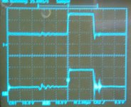
The waveforms tell that your transformer (and your layout?) has huge leakage inductance (the bump in Vds after turn off is tall and long). This leads to excessive snubber dissipation and a loss of efficiency. You should read about low leakage inductance winding techniques (winding splitting and sandwitching is the most straightforward).
The ringing in gate drive waveform after turn off is EMI probably produced by bad layout in general and picked up by oscilloscope probe. Diodes are #1 EMI generators in that kind of power supplies because they exhibit very abrupt impedance changes when they start and stop conducting (series RC snubbers are routinely added in parallen to tame them). Those changes excite the RL tank resonator formed by internal diode capacitance and external lead and wiring inductance resulting in gentle ringing, usually between 10Mhz and 100Mhz (that should be reduced with tight layout and tamed with snubbers).
However, to ensure proper drive, the gate buffers and its supply capacitor must be placed very close to the MOSFET. The collector of the PNP turn-off transistor should be connected directly to the source terminal with a very short wire, and the input filter capacitor ground and control IC ground should be wired to the source terminal too (in a star fashion). Breadboards are not that bad, you can get little parasitistics if you lay out them properly.
Try increasing gate resistor to slow down transients.
Hello again!
Thanks Electrone and Eva, it’s been a pleasure hearing from both of you, too! Thanks so much for the advice, I hope I am not boring either of you
So… today I added the current limiting. It turns out, though, that the circuit I found in the app note does not work! It simply latches the DTC pin to Vref right away, and stays there. Because of this, I designed my own circuit instead. It is a bit more complicated, but it works and makes sense to me. From the new schematic, pin 4 will follow the soft start through D8 while C2 charges. If an over-current condition occurs, Q5 will switch on, pulling the base of Q8 low. With Q8 off, Q7 turns on through R12 and pulls DTC to Vref. Also, Q6 is turned on through R12+R14, which keeps Q8 off even if Q5 turns off. This condition is cleared at the start of each oscillator cycle by D7 (FR103 has a low enough Vforward, around 0.45 volts). I have tested this by triggering Q5 manually, and the circuit seems to work fine.
I have also changed the gate drive method, as per Eva’s first suggestion – I assume this is what you were suggesting. The TL494 output BJTs (paralleled) now provide active turn-on, and the passive turn-off is from resistor R20. This is still buffered through Q1/Q2… is this what you intended? Unfortunately, I could not find any examples of a TL494 driving a mosfet directly… all BJTs or dedicated driver chips. Using this, the gate waveform now looks a little cleaner, and rise and fall times are now 180ns and 155ns respectively. I did not get a chance to try changing the rise/fall times separately using a diode/resistor scheme, I will try it next time. C9/R19 are correct… I actually forgot to change the values on the previous two schematics.
Now, all that is left to rewind the core to reduce my losses there (and do the final PCB construction). Sorry to make you spell this out, but I want to be sure about the winding process:
(1) I think I will wind the secondaries bifilar with smaller wire this time, even though I have suitable wire for a single-conductor secondary. I am hoping to improve coupling here. Good idea?
(2) Also, you mention splitting the primary and sandwiching… I’ve found an excellent document about transformer design:
www.irf.com/technical-info/appnotes/an-1024.pdf
I have previously calculated 8T primary, and 5T per secondary, and I plan a 50/50 primary split as shown. However, I have read elsewhere that I might be able to reduce leakage inductance further by using a non-50/50 split… is this true, and if so, is it worth trying? Thanks again for the fast and helpful responses!!
Attachments
Thanks too. One thing I don't like about the TL494 are the incomplete totem poles on the outputs. I'd rather have the pull down signal amplified internally than the turn-on. When I saw your first circuit it didn't strike me how there would be a delay between the first output turning off and the second turning on in order to turn off the MOSFET. Then there would be the timing consideration to insure that pull down is always completed every cycle.
I have a hard time seeing your diagram because of my weak eyes. Windows refuses to let me save it in another format (actually at all) so that I can use paint to compress it and increase the component size/space ratio. But I don't want you to go through any work messing with that because I have almost no real life experience with the chip. I do almost everything in my circuits with the simple 74C14. It has almost no "black box" aspect, so I don't have too wonder if it is capable of something. The only thing I regret is that National Semiconductor sold their manufacturing operations of the 74C14 and it was immediately degraded in quality.
I have a hard time seeing your diagram because of my weak eyes. Windows refuses to let me save it in another format (actually at all) so that I can use paint to compress it and increase the component size/space ratio. But I don't want you to go through any work messing with that because I have almost no real life experience with the chip. I do almost everything in my circuits with the simple 74C14. It has almost no "black box" aspect, so I don't have too wonder if it is capable of something. The only thing I regret is that National Semiconductor sold their manufacturing operations of the 74C14 and it was immediately degraded in quality.
I don’t mind the uncommitted outputs on the TL494 that much, since they do give you a little flexibility over some other chip designs I’ve seen. However, that being said, they can be a pain to work with. Forgive me if I’m repeating things you already know, but here is my take on it:
The TL494 has two output modes. In the first (the one used in my initial schematic), each output switches ‘on’ separately through the flip-flop action. This mode is really intended for push-pull designs, with two output switching elements. The problem, as Eva identified, in using it in the manner I had shown, is that both pulse widths still track the feedback. So, unless it was running at maximum duty cycle, there could be significant lengths of time where neither 494 output was actively ‘on’, and thus the gate drive was floating (by luck, to an ‘off’ state).
The mode I am using now has both outputs switched at the same time, which requires either a passive turn-off or passive turn-on. So, are you suggesting I should switch it to active turn-off from active turn-on? My fall times are already faster than my rise times… or, are you more worried about false triggering?
Sorry for the cramped nature of my diagrams, I am trying to work within the forum’s image size guidelines. I’ve attached the full size .bmp and ExpressSCH file in a .zip this time.
Attachments
Ahh, I can see it now.
With the pull down resistor, the maximum efficiency is limited because the power dissipation is greatest at turn-off. If the value of the resistor is small enough, the frequency is low enough, or the power output is scant enough, it's OK.
I was thinking of false triggering too. The first diagram appeared to need to juggle the requirements of turn-on and turn-off, which the chip would not know you need to be different; so you would be trying to build circuitry just to fool the chip. Then as you aptly mentioned, the chip would be in the dead time state, leaving the MOSFET gate in limbo.
It's OK about the diagrams' size. It is not so much the cramped nature I have trouble with, which, in fact, I am actually notorious for, it is the small component size and resolution.
You may have picked up on the fact that I have not commented on transformers. It is another peculiar area for me. I don't like to spend a lot of time on strict requirements for them in my circuits, so I prefer to try to make the circuit able to use ones which are not particularly constructed with care. A really well-made transformer can only be practically made with factory equipment. For example, it simply isn't possible for us to make a small signal coupling E-I core transformer, nor out of a toroid for that matter, considering how it requires at least hundreds of turns of fine wire.
Increase the value of the snubber cap C5 to around 100..220 nF (mylar or polypropylene), and see if that reduces the Vds ringing on the switching FET.
You may also have to snubber the secondary rectifiers to reduce ringing - there's probably a fair amount of leakage inductage, some of which is reflected back to the primary.
You may also have to snubber the secondary rectifiers to reduce ringing - there's probably a fair amount of leakage inductage, some of which is reflected back to the primary.
Electrone: I have to agree with you on the transformer – next time I may try a topology where the transformer is less critical. In fact, it took two tries to get a better transformer for this one. The first one actually turned out worse than my original transformer… I couldn’t even set the air gap properly. The second one turned out well, though.
Unfortunately, when I tried switching to an active turn-off drive setup as you suggested, I was not able to reach the performance I had previously. Either the drive became highly dissipative or the turn-on/off delays increased. I suspect with some extra work I could fix this, but the current drive arrangement is working fine for me. I will have to pay careful attention to noise, and component placement, as you and Eva suggest, though.
Linuxguru: I came to this same conclusion at almost the same time you posted the suggestion! Actually, I had to change the snubber values anyway for the new transformer. The new values are 1.5K and 200nF, although these may change once I move off the breadboard. I suspect most of my remaining losses are due to layout – I will post a picture of my setup sometime before I take it apart… it’s certainly set out for my convenience, not for performance
I am still undecided on snubbering the secondary rectifiers – I have tried it before at various points in the development, including on the latest circuit. So far, I haven’t been able to generate an improvement in the ringing without significant extra dissipation. I will post a new Vds waveform sometime soon, the ringing is now down to a single pulse of about 20V magnitude on moderate to heavy loads (36W+). This is well within the mosfet's safe limit. I will, however, give it one more try with the final design. My final stats for the breadboard prototype peak around 72-74% efficiency. I will measure the final numbers, as well as load/line regulation, etc, from the finished circuit. Thanks again everyone!
Terran, I commend you for getting the transformer improved. I have read, even, of a method of placing windings inside a braided shielding sleeve. I had one transformer blow up (rather figuratively speaking), however by winding turns bifilliarly. It is important to consider voltage between windings in that case, I guess, and whether the dielectric strength of the wire insulation is high enough.
I tend to think that at the power level you are targeting, the turn-off approach you have is good. It wouldn't help a whole lot to turn it off faster just to have to snubber it more.
I tend to think that at the power level you are targeting, the turn-off approach you have is good. It wouldn't help a whole lot to turn it off faster just to have to snubber it more.
Sorry for the delay in posting, but I have been quite busy! Thanks for the compliment too, Electrone! The final transformer I used isn’t wound bifilar, that one was the one that turned out the worst. I agree with what you’re saying, and I think I should add that the construction (in terms of consistency of windings, length, tightness, angle, etc.) becomes even more important, especially with bifilar, it seems. My best results were simply from winding half the primary turns, leaving the extra wire at the end of the bobbin, winding the secondaries (stacked, rather than layered, since I had the room), and then winding the other half of the primary turns back down the bobbin using the wire left hanging previously. I realize you probably know this, but for anyone else working on a flyback for the first time, this turned out be the easiest and most reliable method that I found.
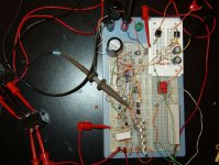
Anyway, here is the promised picture of the breadboard setup in all its horror. The final results confirmed my suspicions that most of my remaining losses were from here. For anyone interested, things *not* to do that you can see in the picture include: long clip leads to the transformer, under-sized wire, electrically poor layout, etc, etc.
That being said, my final product was much, much better. The final stats are as follows:
Vin = 34V to 40V (after input bridge)
Vout (No load) = +18.51/-18.44V
Iin (No load) = 0.045A @ 38V DC
Efficiency = 80.5% (Vout = 36.8V, Rload = 51ohm, Vin=36.15V)
fs = 64.4 KHz
Line Regulation: Not measured
Load Regulation: 0.11% (Vin=38V before bridge, Iout=0.228A to 0.721A)
Output Ripple: <200mV P-P (Issues with the scope on this one, couldn’t get a good measure)
Efficiency hits 80% at around a 450mA load, and hovers there out to at least 2.6A, the largest load I tested. Lowest efficiency measured was ~65% at a load of ~150mA. Voltage output is stable even with a very, very small minimum load (though I suspect the side of output outside the regulation loop could creep up over time with no load at all).
Attachments
- Status
- This old topic is closed. If you want to reopen this topic, contact a moderator using the "Report Post" button.
- Home
- Amplifiers
- Power Supplies
- Noise from TL494 Flyback supply