this stuff is covered by beTheSignal.com
need to register but free content: partial mutual inductance of leads, vias, optimum bypass geometry, plane capacitance...
need to register but free content: partial mutual inductance of leads, vias, optimum bypass geometry, plane capacitance...
That's one of the beautiful things about audio. Getting something working is easy. Then there's a large number of additional refinements, most of which are minor when considered individually. But they somehow add up to noticeable differences rather quickly. And the range in which measured improvement ceases to be audible is not well characterized. Makes for some quite interesting engineering.But when I first started thinking about audio circuits and systems, I assumed that it would all be relatively trivial, because the frequencies are so low. I was wrong. And seeking the difference between "good hi-fi" and "exquisite hi-fi", and how to implement the latter, can be very challenging.
On the commercial side Gold Phoenix is pretty hard to beat. On the DIY side, look at toner transfer etching---with a laser printer, cheap laminator, and some practice you can hold 20 mil DRCs (maybe 15) and about 20 mil registration between the top and bottom of a piece of FR4. I've never laminated boards together to make a DIY four layer because drilling holes and dropping wires through them to create vias seems to make accessing inner layers problematic no matter how you go about it. Someone may have come up with a clever solution for this since the last time I searched. There's probably also someone out there who's got a DIY process for plating vias (though, personally, my living arrangement is such that it's more cost effective just to pay Gold Phoenix).Any thoughts on how to take best advantage of planes, for audio, if I do try it?
In terms of layout, there are two main design pivots; single supply versus dual supply and single ended feedback versus differential feedback. The way I tend to think about it is that FR4 comes with copper on both sides for a reason---if you're not using most of that copper then your layout's probably not what it could be.
With single supply you can usually do a pretty good job of the pours in two layers without too much fuss if you've got your floorplanning decent. With dual supply more creativity's required and I've usually had to work the design quite a bit to get good two layer pours. Either way, the planes get disrupted by signal paths so the supply net lengths are longer in terms of squares than if the planes were poured through in a four layer board. You never get an ideal pour in four layers due to via disruption so, in my experience, the net penalty for two layers is usually somewhere around 10 squares. That's actually not bad; one ounce copper is 0.26 mOhm per square and pours wider than 300 mil (on typical 62 mil FR4) tend to come in around 1nH per square. That's order of magnitude lower impedance than typical audio routing using traces, often well on the way towards two orders of magnitude.
Single ended versus differential feedback is more a matter of perception than anything else. A good differential feedback layout puts the feedback resistors and filter caps close to the control circuit (typically an op amp in line level implementations or discrete in a power amps, though there's really no reason not to use op amps to control solid state power amps too). This minimizes the extent of high impedance (and therefore noise susceptible) trace and hence the amount of noise pickup on the op amp's summing junctions. Of the other four terminals in the feedback network, two are the balanced input and two are the Kelvin sense traces tapping in to the amp's output connector. One's then free to pour planes up to, around, and even underneath the feedback traces---edge to edge coupling's relatively weak and the differential topology's common mode rejection mitigates broadside coupling (at least if the plane's poured consistently through underneath). A good single ended feedback layout looks much the same, just without the resistors on the ground connections. From a topology standpoint there's no difference between this and star ground; it's just a layout adjustment which makes better use of the copper available on the board.
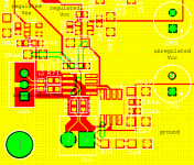
The attached is a two layer example from a board I'm working on a the moment. It's a differential input, single ended output, 500mW composite amplifier channel. U63's the controlling op amp, J65 is the input connector, U65 is the output device, and J66 is the power connector. The regulated pours here aren't ideal. For the lowest inductance they should be underlain with ground on the bottom side rather than the unregulated Vee pour. Or perhaps regulated Vcc and Vee should paired. However, the board's rather small and hence the backside area's wanted for cooling of the 8-PSOP output devices. I'm not entirely settled on the geometry tradeoffs for the regulated planes, which is the main reason the board's not done yet, but my experience is this is mostly splitting hairs---the controlling op amp runs in class A so the regulated supply impedance isn't so critical.
Same one as I talk about over here; in the attached example it'd be U63 and its feedback network. To summarize stuff I've posted on elsewhere in DIYA, THD is a subset of IMD and IMD is be well correlated with percieved audio quality via the Rnonlin metric. To leave tube amps aside for the moment, this means one can use THD as a predictor of audio quality (provided other conditions are met, such as slew rates being high enough to keep the feedback loop closed). Power devices typcially have about 70dB PSRR and an open loop THD around -45dB (that varies with load; the lower the load impdedance, the worse the linearity). If you go back the ripple to signal ratio graph in that post I just linked there's that brutal range at the low power end of the graph where the ripple amplitude is 40dB or more above that of the output signal. The open loop output error will therefore be dominated by ripple leaking through the PSRR, creating some sort of THD/IMD/noise floor at -30dB.Which "control loop"?
A reasonable rule of thumb is artifacts 50dB below signal are audible to critical listeners, with the threshold of inaudibility being somewhere around -60dB (Ethan Weiner arrived at this first but I came to it independently). Since distortion from good drivers is about -60dB it can be desirable to hold the electronics' nonlinearity well below that in order to keep playback fidelity limited on the drivers. This suggests the electrical THD/IMD/noise floor should be around -70dB, perhaps -80dB to have some margin for the unexpected (or for Ethan and I perhaps having bad ears
") ). Using a regulator with 50+dB ripple rejection on the output devices' supply will get the ripple out of the way, but one's still stuck with the -45dB floor from the nonlinearity.
). Using a regulator with 50+dB ripple rejection on the output devices' supply will get the ripple out of the way, but one's still stuck with the -45dB floor from the nonlinearity.This means you need a control loop to linearize the output. Since the ripple is 40dB above signal and we want to linearize to at least 70dB below signal, the control loop requires a PSRR of 40 + 70 = 110dB. Minimum. 120dB+ is preferable. It's extraordinarily difficult to hit this in discrete. Good op amps will do it at low frequencies but not at 20kHz. So either you need an insane power supply with something like a Farad of low ESR and low ESL caps or you regulate the control loop supplies. The latter approach is much cheaper, easier to build, and decent choice of regulators will give you 50dB ripple rejection at 20kHz. Combine that with an op amp's PSRR and you get 140+dB, enough to push the THD/IMD/noise floor down to -110dB. If you want to. Most control loops don't have sufficient excess gain to do so, but that's a separate discussion.
Mainly works with rectangular caps that are long side adjacent over planes. The required geometry's obvious if you can visualize the electromagnetic fields in whole structure but I don't have good link handy to help with that. Perhaps jcx's link has the goods---haven't looked.It might also only or mostly apply to MLCCs, with the layers aligned correctly.
Oh, there's more coming, no worries about that. This project's looking like it's gonna have a 2.17GHz VCO in a 32-QFN; the supply for that's really quite fun.Yes, I could definitely enjoy it if you and marce did another couple of hours' worth!
Attachments
Last edited:
Alt+0233It is clear from your expose (how does one add a ' above an e to make it sound A) that distance has a very big role in effectiveness of decoupling.
é
How thin does the FR4 have to be? Would it have to be 20 mils or would thicker still be beneficial enough?
the resulting fast current slew rates should not have to be seen by the supply (which is a good thing, especially if the rails have any length to them, since their inductance would probably then cause a very large ripple voltage). THAT'S EXACTLY why the decoupling caps at the point of load need to be able to do it! That's basically been my main point, here, all along. i.e. I have been trying to figure out how to select the decoupling caps and how to position them so that even the inductance of their own local connection to the load (and with all of the other parasitics) doesn't make it impossible for them to deliver the worst-case transient current waveform with precise accuracy of timing and amplitude.
Cheers,
Tom
Tom,
As far as my experience goes (with analog) there's usually too many voltages to decouple and not enough layers or board area to make a power / ground plane capacitors. You really only start to get some significant benefits when the planes are separated by 5mils or less (~200pf/in^2).
However with local planes around the component(s), even with 20mil separation, as already mentioned you can get the inductance low and comparable to the package inductance, allowing you to add additional capacitors further away.
I appreciate your efforts to characterize what impedance is needed for the supplies, including up to the full bandwidth.
Thanks
-Antonio
5mils (0.005") & 20mils (0.02") !
Are we to start designing >4layer boards to take advantage of the ground planes that we don't yet know how to design for audio frequencies?
1mm PCB is ~ 40mil and 1.6mm PCB is ~ 60mil.
Andrew,
As far as I see it's rather converging that for Audio frequencies and the bandwidth required to support them, there is no real benefit with many of the techniques being discussed and used in the high speed digital arena.
If the requirements are such as to maintain an impedance below some maximum out to 20Mhz then discrete well placed combination of capacitors should suffice.
However for me personally since I make very few boards (~1 a year) the extra cost for a 4 layer allowing for some planes affords me lot more flexibility to implement the required capacitors as well as providing a low impedance reference for the remainder of the board.
Thanks
-Antonio
AndrewT said:Where can I find a table of these other symbols/letters when "insert" is not available?
Hi,
Here: ASCII Code - The extended ASCII table
5mils (0.005") & 20mils (0.02") !
Are we to start designing >4layer boards to take advantage of the ground planes that we don't yet know how to design for audio frequencies?
1mm PCB is ~ 40mil and 1.6mm PCB is ~ 60mil.
I think that I will probably at least try four layers, just for the sake of a much better layout, and in order to have a ground plane or two, and to have power planes (or planes of power and signal). Even if the capacitance between layers isn't significant, the inductance of the ground connections should be lower than otherwise.
The only serious drawback that I can think of for DIY, off hand, is that through-hole components would be problematical, in most cases, unless access holes were made in the outer layers for hand soldering on inner layers. But maybe access holes would work OK, for the large-pitch devices that people here often work with, and especially with thin boards and layers.
Looking at Henry Ott's book, for a four-layer board I rather like the idea of ground on the outer two layers and signal+power on each of the inner two layers.
Homemade versions of those could also be done, with two double-sided boards and an insulating sheet. But it would be a lot different than a layout for a fab house so that in general a layout for a professional fab job usually could not be adapted to the type of home made process that I'm thinking about, unless the designer took the time to make it so that it could, assuming it was possible.
What I would probably do is surface-mount as much stuff as possible. And for DIY I think that just about any through-hole part that has flat pins that are near the edge of the part could also be used as a surface-mount part (and maybe even many leaded parts as well).
Wow, imagine not having traces or pins always in the way at critical points, when routing a board!
On the other hand, for most chipamp boards, the layout might be improved enough just by using a two-sided board with one side as a ground plane.
ΘΘdefg╚,É⌠X╝ ääé
AHH!
"Alt" + 0233 on the numbers keypad gives é
Thankyou.
Where can I find a table of these other symbols/letters when "insert" is not available?
How can I make Alt-181 produce the "micro" sign instead of ╡, which on my screen looks like a vertical bar with two line segments protruding to the left, near the center? Is it just a matter of selecting a different font (which I also can't seem to do, at least not for "window" text)?
Last edited:
How can I make Alt-181 produce the "micro" sign instead of ╡, which on my screen looks like a vertical bar with two line segments protruding to the left, near the center? Is it just a matter of selecting a different font (which I also can't seem to do, at least not for "window" text)?
I wonder that myself given the table I linked to. Although, straight from my memory; alt + 230 = µ
µ
Woo hoo!! µF!!
±√(b² - 4ac)! ≤ ♪ ♫
This chart seems to be correct, but not complete:
Extended ASCII Display Characters
Woo hoo!! µF!!
±√(b² - 4ac)! ≤ ♪ ♫
This chart seems to be correct, but not complete:
Extended ASCII Display Characters
http://www.linearaudio.nl/Miscellaneous/bypass_capacitors_part1.pdf
http://www.linearaudio.nl/Miscellaneous/bypass_capacitors_part2.pdf
http://www.linearaudio.nl/Miscellaneous/bypass_capacitors_part3.pdf
http://www.linearaudio.nl/Miscellaneous/bypass_capacitors_part4.pdf
http://www.linearaudio.nl/Miscellaneous/bypass_capacitors_part5.pdf
http://www.linearaudio.nl/Miscellaneous/bypass_capacitors_part6.pdf
Last edited:
Mostly in the right direction, though there are a few errors like the trace resistance and inductance being in parallel (how'd they miss that one?) and the assumption op amps operate in class B. You'll find many of the same issues arise in switchmode supply design. Basically it's a tradeoff between supply performance and the supply phase yo yoing from capacitive to inductive---the lower the ESR, the lower the supply's self induced ripple but the greater the phase swings.
The table is too big to fit on a "post it", stuck to the side of my 27" monitor !
How the .... do we oldies remember all those ascii codes?
BTW,
I have down loaded those ascii codes before, but I can't remember where I saved them !
How the .... do we oldies remember all those ascii codes?
music to your ears?≤ ♪ ♫
BTW,
I have down loaded those ascii codes before, but I can't remember where I saved them !
Last edited:
I have read this three times now........... it's a tradeoff between supply performance and the supply phase yo yo-ing from capacitive to inductive---the lower the ESR, the lower the supply's self induced ripple, but the greater the phase swings.
I think someone will have to help me through understanding the message therein.
Mostly in the right direction, though there are a few errors like the trace resistance and inductance being in parallel
I believe these parallel resistors are modeling skin effect losses (there is also a series R, at least in the figures I saw).
I havent read through all these articles but am looking forward to, thanks for posting them. I think this get covered some but it still seems to me that despite getting fairly complicated simulation circuits the hardest part is what Gootee is attempting to do which is to determine the required minimum impedance throughout the entire frequency range, not just audio.
Thanks
-Antonio
- Status
- This old topic is closed. If you want to reopen this topic, contact a moderator using the "Report Post" button.
- Home
- Amplifiers
- Power Supplies
- paralleling film caps with electrolytic caps