When bypassing with low value, low esr capacitor it will only "throw" the noise back and forth between rails, so its better that the noise get dissipated somewhere like with a snubber together with the bypass capacitor. Like IRF does with their amp, 100nF bypass and 100nF + 1 ohm snubber.
Schematic on page 30 (C13+R31/C14+R32)
http://www.irf.com/technical-info/refdesigns/iraudamp4a.pdf
And i see on page 29 they use 100k resistors (R57, R58) between the rails to ground together with the 1000uF electrolytes. High frequency noise have no current (Ampere) potential, and will be dissipated by the 100k resistors.
Hope that helps") (correct me if im wrong)
(correct me if im wrong)
Schematic on page 30 (C13+R31/C14+R32)
http://www.irf.com/technical-info/refdesigns/iraudamp4a.pdf
And i see on page 29 they use 100k resistors (R57, R58) between the rails to ground together with the 1000uF electrolytes. High frequency noise have no current (Ampere) potential, and will be dissipated by the 100k resistors.
Hope that helps
(correct me if im wrong)Hello,
Francis Ibre a very respected and famous audiophile in France explain that bypassing PSU electrolytics with film caps is a very good thing for sound quality but he laughs when he see schematics with little values (often less than 1uf). He says that to have serious effect you have to increase the value up to 20uf. I tested 2uf mkp capacitors and the quality of the music increased (more "airy") when I replaced it with 20uf mkp... whow it seemed like I changed the amp! The increase in quality was unbelievable!
You can thind on Ebay 20uf MKP for about 5 euros
You could always try some of these:
http://www.wima.com/EN/WIMA_DC_Link_HC.pdf
JK
Large physical size should be avoided as much as possible, if not ESL is low.
Bypass film caps should be a larger value i think too, but i would not feed it with ac current when its purpose is to deliver ac current for the output. So i would use snubbers to get rid of frequencies above desired output bandwidth placed between the bypass film cap and electrolyte caps. And high value resistors in parallel with the electrolytes like IRF does, because electrolyte is too big physical (ESL) together with too high ESR to bypass high frequencies.
After doing a bit of research...
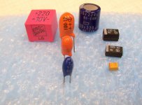
C1 - C4 - WIMA MKM4 1.0uF 250V
C5 - C10 - 1000uF 200V Nichicon KX
R1 - R4 - 3.3Ohm 5W Non Inductive
C11 & C12 - 2200uF 250V Panasonic TUP
L1 & L2 - 10mH 20A JW Miller Choke ( 5522RC )
The Cap Bank will be on a separate board and its gonna have 4 x 2.2uF 850V EPCOS Snubber Film Caps at the input and output of the cap bank which will be comprised of 12 x 10000uF 100V Chemi-Con KMH caps
An externally hosted image should be here but it was not working when we last tested it.
C1 - C4 - WIMA MKM4 1.0uF 250V
C5 - C10 - 1000uF 200V Nichicon KX
R1 - R4 - 3.3Ohm 5W Non Inductive
C11 & C12 - 2200uF 250V Panasonic TUP
L1 & L2 - 10mH 20A JW Miller Choke ( 5522RC )
The Cap Bank will be on a separate board and its gonna have 4 x 2.2uF 850V EPCOS Snubber Film Caps at the input and output of the cap bank which will be comprised of 12 x 10000uF 100V Chemi-Con KMH caps
Snubbers with 1000uF capacitors will filter away 50hz into the resistors, making huge waste of power. 1uF maybe? Snubbers are there to remove transients, but in case of IRF amp its there to lower transients in supply voltage coming from buspumping in the output stage.
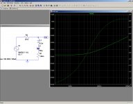
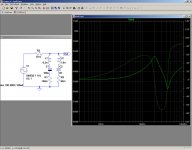
I did some simulations on powersupply with 50hz ac, and it seems like adding those 100k resistors at the electrolytes is a bad idea. Because they constantly draw currents from the electrolytes, and makes more noise in the supply voltage. So i would put the resistors and snubbers before the rectifier or transformer. Putting inductors in the curcuit with simulator made more noise also. Dont know how reliable simulator is, any comments?
I did some simulations on powersupply with 50hz ac, and it seems like adding those 100k resistors at the electrolytes is a bad idea. Because they constantly draw currents from the electrolytes, and makes more noise in the supply voltage. So i would put the resistors and snubbers before the rectifier or transformer. Putting inductors in the curcuit with simulator made more noise also. Dont know how reliable simulator is, any comments?
Some more material:
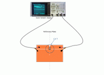
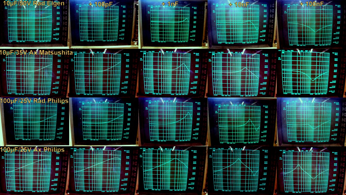
Here are some actual and systematic data on the subject of paralleling a small ceramic cap (100pF - 1nF - 10nF - 100nF) with various types of electrolytics.
These are impedance plots between 0.3 and 100MHz, and in this particular set-up, the 0dB level is equivalent to 37.5 ohm.
A short executive would be: another myth is gone.
Basically, all the serious guys (and gal) in this thread are right.
A complete description of the test set-up and methodology can be found here (in french):
Tout ce que vous avez toujours voulu savoir sur les condensateurs de découplage sans oser le demande - Forum Électronique
Attachments
-
 CapTestSetUp.GIF40 KB · Views: 2,108
 -
 Parade.jpg114.9 KB · Views: 2,085
 -
 TestJig.jpg155.5 KB · Views: 2,067
 -
 CapTExample.gif114.5 KB · Views: 1,949
 -
 Concept1.jpg166.8 KB · Views: 1,007
 -
 Concept2.jpg179.2 KB · Views: 842
 -
 Cap Data3.jpg342.2 KB · Views: 698
 -
 Cap Data2.jpg328.6 KB · Views: 1,048
 -
 Cap Data1.jpg316.7 KB · Views: 1,070
 -
 Cap Data4.jpg363.6 KB · Views: 650


do those results show that there is insufficient damping of the two //cap resonances in the esr inherent in the two caps used for each experiment?
If more damping resistance is required, where should it be placed? In the path of the big electro and/or in the path of the smaller HF bypass?
If more damping resistance is required, where should it be placed? In the path of the big electro and/or in the path of the smaller HF bypass?
The subject is not simple, and I remember Eva had given valuable advice about it, in this thread or in another one.do those results show that there is insufficient damping of the two //cap resonances in the esr inherent in the two caps used for each experiment?
If more damping resistance is required, where should it be placed? In the path of the big electro and/or in the path of the smaller HF bypass?
But basically, in most case, bypassing directly (locally) the electrolytic is not only useless, but harmful most of the times.
If damping has to be added, it has to be either in series with the small one (0.47R f.e.), or to be a RC network of his own, added to the two paralleled capacitors.
Here is the post (or one of them) in question:
http://www.diyaudio.com/forums/powe...ing-psu-capacitors-effective.html#post1566979
http://www.diyaudio.com/forums/powe...ing-psu-capacitors-effective.html#post1566979
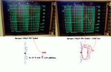
According to this plot, 10uF electrolytic paralleled with 100nF ceramic doesn't look bad at all, could this sort of combination be a more practical bypassing scheme to play with?
It would be interesting to repeat the experiment with much larger value shunt film caps and see whether the behavior is similar. I suspect it is nowhere as extreme, but may in fact sometimes occur in a frequency range where it might be audible.
A very small ceramic cap with its very high Q (low esr/esl) is not the sort of thing I would put in parallel with a large inductor, err electrolytic cap - something with a much lower Q might provide better results and something with an appreciably higher capacitance might decrease ESR slightly at higher frequencies.
IMHO the 100nF plot doesn't look all that good to me, and without a network analyzer it would be hard to tell if you made things worse. Bypassing AL electrolytics directly with ceramics is not good design practice IMHO.
I'm just curious, I generally don't bypass electrolytics in power supply applications for this and other reasons.
[Should be a new thread, maybe?]
Yeah, I think there's no use in beating that dead horse, any more (except, of course, for the sheer joy of it): Small-value bypass caps on the large smoothing caps in a power supply are either useless or dangerous.
It might be useful to put some damping at the rectifiers, if there's ringing. But that would be done with resistors and any caps involved would only be in series with the resistors to limit dissipation at non-problem frequencies. (But, of course, if the caps ESRs were the correct resistance, we could kill two birds with one stone. [See below for how to determine the optimal R value needed to damp any ringing, basically anywhere.])
This is pretty darn interesting:
http://www.diyaudio.com/forums/powe...ing-psu-capacitors-effective.html#post1566979
But that basically assumes that the large cap is already right at the point of load (so no supply-rail inductance remains).
*** Getting the point-of-load bypass/decoupling cap(s) situation optimized is now the more-important thing to be investigating (for the purposes of the topic of this thread, at least).
Supply-rail conductor inductance, between the main smoothing caps and the point of load, is one of the main reasons that bypass/decoupling capacitors need to be used at the point of load. But that stray inductance can also form resonances with the capacitances used, as can the parasitic inductances of the other caps, if caps are paralleled at the load.
Parasitic or "stray" inductance and capacitance (and the resonant "tank" circuits that they can form) are, in general, what need to be tamed, wherever we don't want resonances, which can cause ringing, instability/oscillation, spikes, reflections, etc, depending on the type of circuit.
Using a shunt resistance that is equal in value to the characteristic impedance of the resonant circuit formed by the capacitance and inductance will optimally damp the unwanted resonance.
Then, if the power dissipation in the resistance would be too high (presumably due to working frequencies that are not near the unwanted resonant frequency), then a capacitor is added in series with the resistor, to form a "snubber", so that only the frequencies that need to be damped have to be dissipated in the resistance that is needed. (See. No magic.)
Below I have paraphrased a procedure from a Maxim appnote that describes a practical method for easily determining the optimal snubber/damping/termination resistance value (and snubber capacitance value, if necessary).
The method, as given, assumes that only parasitic (i.e. "stray") capacitance and inductance are present, as might be the case with an FET gate circuit, or a transmission line (e.g. LVDS or other signal or power buss). But if there is a known L or C in an existing circuit, that should just make the method even simpler to apply.
The method requires an oscilloscope, or some method of measuring the frequency of ringing or oscillation that is occurring (or that can be forced to occur, for this purpose).
Basically, if there is no L or C component (only parasitics), and there is ringing (or if you can inject fast-edged pulses through an R and create ringing), or "reflections" in the case of some transmission lines or busses, then you can insert a capacitor of a particular value such that the ringing frequency is halved. If you work out the math, the C value that halved the ringing fequency is 3X the value of parasitic capacitance that is involved.
Knowing the parasitic C and the ringing frequency, you can then calculate the parasitic L (see below).
And knowing the C and L, you can calculate the characteristic impedance, R (see below).
You then use that R as the damping or snubbing resistance (or as the buss-termination resistance, as the case may be), and if necessary use 4X to 10X the parasitic C in series with the R, to limit power dissipation in the R.
If you already have a capacitor present, such as might be used on a power rail (buss), and if the ringing frequency is known (measured), then you wouldn't even have to experiment to find the C and could immediately calculate the parasitic inductance and then the characteristic impedance, and get the optimal value of damping resistance needed. For ringing frequencies outside the audio band (assuming we're talking about an audio amp power rail), then a capacitor would probably be inserted in series with the R, to limit unnecessary dissipation of lower frequencies.
Here is the method, as I paraphrased it from CCFL Push-Pull Snubber Circuit - Maxim :
-------------------------
Below is a pretty slick and practical way to determine parasitic capacitance and inductance, and the characteristic impedance and optimal damping or termination resistance (and snubber capacitance) needed when ringing or reflections (as the case may be) are present.
This is a very simple method for determining the parasitic capacitance and the parasitic inductance that are causing a resonance in a circuit or a transmission line or PCB trace, which also gives the characteristic impedance for the resonant circuit, which is everything needed in order to damp, snub, or terminate it, optimally.
This assumes that there is a ringing condition, already, such as might occur on a digital buss or a transmission line or PCB trace, or at an FET gate, or in a switch-mode power supply, or even an AC-to-DC transformer/rectifier circuit, and in many other types of circuits. (If you don't have ringing and just want to determine the values of some of these parameters, I guess maybe you could try hitting your circuit with a pulse train until it rings.)
1. Measure the frequency of the resonance or ringing voltage, using an oscilloscope.
2. Add a shunt capacitor and adjust the value of this capacitor until the frequency of the ringing is reduced to half of its original value. The value of this resulting capacitor will be three times the value of the parasitic capacitance that is involved in creating the resonance condition.
3. Because the parasitic capacitance is now known, the parasitic inductance can be
determined using the formula:
L = 1 / [{(2 x Pi x F)^2} x C]
where F = (original) resonant frequency and C = parasitic capacitance.
4. Now that both the parasitic capacitance and inductance are known, the characteristic impedance of the resonant circuit can be determined using the following formula:
Z = SQRT(L/C)
where L = parasitic inductance and C = parasitic capacitance.
5. The resistor for the terminator or for the RC snubber circuit should be sized to be equal to the value of the characteristic impedance, Z, and the capacitor should be sized between four and ten times the parasitic capacitance. The use of larger (than 4X) capacitors slightly reduces the voltage overshoot at the expense of greater power dissipation in
the resistor.
An R alone would work to prevent or damp-out the ringing (or reflections, as the case may be). But if power dissipation in the R would then be too high, a C is added in series with the R, so that only unwanted frequencies have to be dissipated in the R.
-----------------------------------------
The following is also interesting but note that it is primarily aimed at someone designing a higher-frequency circuit. However, keep in mind that audio circuits have many potential high-frequency issues.
http://www.analog.com/library/analogDialogue/archives/39-09/layout.html
Cheers,
Tom
Last edited:
It is good, for basically two reasons: the 10µ is small, and thus has a relatively large internal resistance (the physical one, ohmic, not the ESR which is tanδ expressed in a different form), hence good damping, and the ratio of the large to the small cap is not too large: 100 in this case: that is one of the rules that can be learned from those measurements.According to this plot, 10uF electrolytic paralleled with 100nF ceramic doesn't look bad at all, could this sort of combination be a more practical bypassing scheme to play with?
If the ratio is kept <100, then the effect is globally positive, provided of course good layout practices are respected: long wires, large enclosed areas can ruin any combination.
wow what a wealth of info and very apt to what i'm doing at the moment. one thing however, i'll have to delve into the info here further, but the measurements so far mostly seem to relate to leaded parts. i'm doing quite a bit of playing with battery power supplies in fairly small areas, can anyone point me to more relevant info? of course the same rules apply. i'm mostly following datasheets recommendations and using the minimum uf at the input and output of the regs with a minimum amount of impedance needed to dampen ringing, but with enough capacitance to provide desired transient response (with LDOs their transient response is mostly a direct function of output capacitance) and a 10nf np0 is recommended to bypass the reference/ADJ pin for lowest noise
Mostly this entails placing 22-100u panasonic SP (special polymer) caps (AFAIK the lowest Z polymer available, with as little as 5mOhms @ 100uf) and closer to the point of load (which is up to about 50-75mm away) i'm placing 100-470nf np0 -10uf x7r or 1u smd pps film. following the datasheet using ceramic caps by themselves can cause ringing if a minimum ESR is not met, so in general keeping damping in mind; a mix of carefully sized polymer and quality ceramic is desirable; I donmt yet have the skill to provide the desired series R by way of trace resistance
but this thread has me rethinking this a little, since the loads i'm powering in general are well decoupled with polymer and ceramic close to/effectively ON the pins. so i guess i'm torn between making this regulator board fairly self sufficient, considering it will only ever be used to power something directly under it, or providing the bare minimum and letting the local decoupling do its job.
my tendency is overkill and thus i provided many optional pads for decoupling which may or may not end up being used, but i would prefer not to do harm.
i will be buying a scope in the next month or 2 and will revisit it then, but just wondering if anyone has any nuggets of wisdom relating more specifically to multilayer smd, battery powered, low noise, fast transient response mixed signal designs where inductance is less (both trace and component) of an issue?
Last edited:
Elvee said:If the ratio is kept <100, then the effect is globally positive, provided of course good layout practices are respected: long wires, large enclosed areas can ruin any combination.
thanks for that, thats what ive been doing mostly as habit and as a result of previous experience and advice. it makes sense too.
Much more data is available in the original (french) article:How could this thread die after seeing such good empirical data?
Tout ce que vous avez toujours voulu savoir sur les condensateurs de découplage sans oser le demande
to simplify the question, given the 100:1 rule is adhered to, is it still best to avoid additional decoupling capacitors on the load line between the regulator and the load; with only minimum output capacitance and let the local decoupling caps do their job? will additional parallel bypass caps add up with the localised caps to trigger unwanted resonance even given the correct ratio using low inductance parts and routing, or will they actually help?
I guess i'll dust off google translate and check out that thread, French translation to English isnt usually too bad.
I really cant avoid getting a scope any longer, this hobby is getting far too serious =)
thanks to all who have contributed to this thread, its a very interesting and often forgotten/ignored subject, with paralleled caps usually thought to be good no matter what
Last edited:
- Status
- This old topic is closed. If you want to reopen this topic, contact a moderator using the "Report Post" button.
- Home
- Amplifiers
- Power Supplies
- paralleling film caps with electrolytic caps