3.9 and 4.1V
3.9V + 4.1V is not 16.5V ???

But, it sounds close to correct
3.9 and 4.1V
That sounds about right.
....I need to put these aside for a while. Too frustrating!
Don't give up yet Ron, your almost there.
....I can no longer get past the slowly re-glowing light bulb on either of the boards....
Thats because your trying to bias the amp with the bulb tester still connected, remove it then re-bias the amp (turn the bias down first before powering up), job done.
Last edited:
Predictably, Itsmee, you are correct. Both boards seem to be working fine. They are mounted in the chassis and have been running stably for 40 minutes.
I think I knew when this build went bad, that it would drive me to the edge before working.
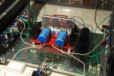
I have begun a final assembly (given this build, probably not THE final assembly) with the BA-3 front end. Picture below.
I have tested each of the BA-3 and F4 channels one at a time and all were stable (950mV for BA-3, 185mV for F4). Connecting them all together for the first time. This should be fun….
I think I knew when this build went bad, that it would drive me to the edge before working.
I have begun a final assembly (given this build, probably not THE final assembly) with the BA-3 front end. Picture below.
I have tested each of the BA-3 and F4 channels one at a time and all were stable (950mV for BA-3, 185mV for F4). Connecting them all together for the first time. This should be fun….
Attachments
 and don't give up the building, you will get a lot of satisfaction from it once you have got over the frustrating bits
Hello,
I would like to share grounding idea of my ballanced f4. Peter Daniel helped me, thank you very much, Peter, so I hope attached drawing will help some of novices too.
Wishing Nelson quick and full recovery,
Andrzej
How do you implement this grounding assuming standard F4 with diyAudio PCBs? Should the ground pin of XLR be connected directly to the ground on PSU board? Or to the ground on one of F4 boards? Or should I introduce another star point somewhere?
I have been listening to the F4/BA-3 for over a week now and am very impressed with the sound. It has stable 200 mV bias and 2 mV offset after playing for hours.
I do have a problem with turn-on though. Two times out of maybe 12 power-ons, both fuses blow. Both times it was first turn on in the morning after being off all night. In both cases, after immediately replacing the fuses, it starts normally.
The fuses are ceramic, 2.5A, slow blow. I have 66K mF per rail and the BA-3 connected to the power supply. I am using SL22-10005 thermistors (10R) and have installed bleeders but do not have a cap across the primaries.
Is this an inrush problem?
Yes sounds like the in-rush current on the power supply. The more caps you have the greater the current spike at switch on.
When you turn it off and then turn it back on in a short period of time the caps still have a lot of charge in them so the in rush current is low, but if you leave it off for a while the caps will completely drain causing the big current spike on switch on.
The Thermistor should help though if you have connected it properly.
Inrush? Yes.
Use 3.0A fuses. If those don't hold increase to 3.5A
Thought so. Will give 3.1A fuses a try.
6L6, you're up early!
Curllian-F4
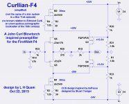
No, it is not the name of a star system in a Star Trek episode. This is a folded cascode preamplifier for the FirstWatt F4 inspired by John Curl's Blowtorch. The simplified design show below is single ended, but it is trivially made into a balanced version.
The design challenge is to get 20 volt peak output with only a 24 volt power supply with low distortion. In a day or two, I will be showing results from a PCB design which "piggybacks" on the Cviller F4 V2.0 board.
It is easy to improve the distortion at high output voltage swings by using a higher voltage supply, such as +/- 36V at 100ma.
Attachments
No, it is not the name of a star system in a Star Trek episode. This is a folded cascode preamplifier for the FirstWatt F4 inspired by John Curl's Blowtorch. The simplified design show below is single ended, but it is trivially made into a balanced version.
The design challenge is to get 20 volt peak output with only a 24 volt power supply with low distortion. In a day or two, I will be showing results from a PCB design which "piggybacks" on the Cviller F4 V2.0 board.
It is easy to improve the distortion at high output voltage swings by using a higher voltage supply, such as +/- 36V at 100ma.
Will the gate voltages of the output MOSFETs limit Vo to 32 V peak to peak ; because Vdg for either will reach 0 V at +/-16 V signal swing?
No, it will provide somewhere around 40V peak-to-peak. Vgs of the MOSFETs is about 4.5V.Will the gate voltages of the output MOSFETs limit Vo to 32 V peak to peak ; because Vdg for either will reach 0 V at +/-16 V signal swing?
No, it will provide somewhere around 40V peak-to-peak. Vgs of the MOSFETs is about 4.5V.
The gate voltages are locked at +/-16 V by the resistor string divider. Each MOSFET has the right polarity for Vds throughout the signal excursion; but Vdg reverses by +/- 4 V. For example; the drain voltage for N20 is always more positive than that of its gate for linear opereation . You are saying that its drain voltage is allowed to be 4 V below that of its gate. It maybe like saying that the voltage at the collector of NPN is allowed to be less than its base voltage, and this bjt still functions as a linear amplifier. A switch?
Look at the datasheet curves for Id vs Vds for the 3N30 and 2N20 MOSFETs. You will see curves for constant Vds gate voltages, showing Vds approaching zero volts. Thus for the Nmos part, Vgd is negative and for the Pmos part, Vgd is positive.The gate voltages are locked at +/-16 V by the resistor string divider. Each MOSFET has the right polarity for Vds throughout the signal excursion; but Vdg reverses by +/- 4 V. For example; the drain voltage for N20 is always more positive than that of its gate for linear opereation . You are saying that its drain voltage is allowed to be 4 V below that of its gate. It maybe like saying that the voltage at the collector of NPN is allowed to be less than its base voltage, and this bjt still functions as a linear amplifier. A switch?
Look at the datasheet curves for Id vs Vds for the 3N30 and 2N20 MOSFETs. You will see curves for constant Vds gate voltages, showing Vds approaching zero volts. Thus for the Nmos part, Vgd is negative and for the Pmos part, Vgd is positive.
Thanks lhquam. Looked at the graphs for 3N30. As you said and that is interesting info I did not know.
I forget to mention two points. It is undesirable to operate the MOSFETs at low Vds because the capacitances increase significantly, thus increasing distortion. To avoid this requires running the folded cascode at higher voltages, requiring either a 2nd (low current) power supply, or a higher voltage supply on the F4 (thus increasing power dissipation). If the voltages on the source pins of the MOSFETs are increased, then the have the problem that the 2SJ74 (and possibly the 2SK170) JFETs are subjected to voltages higher than desirable, which can be solved with cascodes on them. I will soon present a version of the Curllian-F4 that runs with +/-36V supplies and has much lower distortion, particularly at high voltage swings.
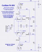
I like your use of Zeners to lower Vds and thus the Pd of the front end FETs. In other threads, DIYers have shown concern about noise from the Zeners. Is this a problem here?Here is the version running on 36 volt rails with lower distortion figures.
Good question. I had not considered that issue in this design, but it is obviously something to consider. Maybe someone more familiar with Zener diode noise issues can respond. The circuit conditions are Zener currents equal to the Idss of the JFETs, somewhere between 6ma and 15ma. Zener voltage of 15V. Preamplifier gain of around 6 or 7 into the F4, which has no voltage gain.I like your use of Zeners to lower Vds and thus the Pd of the front end FETs. In other threads, DIYers have shown concern about noise from the Zeners. Is this a problem here?
- Home
- Amplifiers
- Pass Labs
- F4 power amplifier