Banned
Joined 2002
carpenter said:
Sure, I'd take a chance, but make a subtle change. If things work in your favor, continue--less chance of letting out the magic smoke.
No magic smoke, we don't want that.
Which F4 version do you own?
6/4 Eleanor! (6/4/07 version) The PD boards. BUT it is in pieces at the moment, and with my schedule, will be until right before Christmas.
Magura was one of its midwives but he probably can't give you measurement info unfortunately..
Variac said:
6/4 Eleanor! (6/4/07 version) The PD boards. BUT it is in pieces at the moment, and with my schedule, will be until right before Christmas.
Magura was one of its midwives but he probably can't give you measurement info unfortunately..
Darn...
carpenter said:quite the answer I wanted.
You can put a brick and a piece of metal on a scale and have static equilibrium, that doesn't mean they're the same but only on opposite sides.
Complementary wise, Mosfets are less well matching than Bipolars, and vertical Mosfets are worse than lateral devices.
The reason why some prefer quasi-complementary and Mr Hansen has to go the fully balanced symmetrical way to skip global NFB.
About the static, I am aware and do my best. I make sure to touch ground before picking anything up. I would guess that if I had taken something out with static that it would not be passing a signal and making music. And the identical behavior between the two channels signals to me, in my limited experience, that everything is functioning properly, just that there is a mismatch or imbalance somewhere.
The diodes are correct. 1N4736.
Bias process is as described. Center P2, set P1 to zero. Power it up. Bring P1 up to adjust bias. Voltage across bias resistors to 200 mV per manual. Then adjust the DC offset with P2, measuring between ground and + out.
So far the smoke is still in. I hope to keep it that way.
DaveM said:
Bias process is as described. Center P2, set P1 to zero. Power it up. Bring P1 up to adjust bias. Voltage across bias resistors to 200 mV per manual. Then adjust the DC offset with P2, measuring between ground and + out.
Sounds good to me.
It's when you bring the bias measurement up to 200mV that the offset swings to 30 volts, yes? How far can you adjust the offset with P2?
Edit: how about a close-up pic of your pcb?
The 30 V DC offset is with P2 turned to zero. When I start with it in the middle the offset in higher.
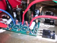
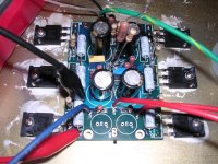
About the picture.... I intentionally left the leads long on all my changed parts. They are RS parts and I plan to change them out with Vishay's once I get it running and the values dialed in. Keeping the questionable components high off the boards makes them a whole lot easier to work with.
About the picture.... I intentionally left the leads long on all my changed parts. They are RS parts and I plan to change them out with Vishay's once I get it running and the values dialed in. Keeping the questionable components high off the boards makes them a whole lot easier to work with.
Attachments
Banned
Joined 2002

There's mica under those fets? Just making sure....
You're certain that your solder/pads are clearing the heatsink? Can you slip a piece of paper beneath the pcb?
Edit: Can you zoom in? Can you get some shots of the FET numbers? Get a few more overhead shots?
Edit: what's that long lead resistor next to P2 doing?
Need a shot of the other end of the pcb.........
Maybe obvious but ...
Picking up on the previous post, with everything off, I'd check for shorts between the legs of the output transistors and the heat sink. Just put your meter on 'continuity test', one lead on the transistor leg and one on the heatsink. If you get a tone, there's a short somewhere.
Though, as you stated before, since the problem is evident in both channels, this is less likely, ...
unless you didn't insulate the output devices uniformly.")
Keep at it, you will find the fault sooner or later.
Ryan
Picking up on the previous post, with everything off, I'd check for shorts between the legs of the output transistors and the heat sink. Just put your meter on 'continuity test', one lead on the transistor leg and one on the heatsink. If you get a tone, there's a short somewhere.
Though, as you stated before, since the problem is evident in both channels, this is less likely, ...
unless you didn't insulate the output devices uniformly.
Keep at it, you will find the fault sooner or later.
Ryan
Iam somewhat confused 
How can you have 30 VDC offset with +/- 23.8 volt rails?
This doesn't seem like it would produce such a large offset.
Is the version you are using have P2, the offset adjust, as 5K or 500 ohms?
The 30 V DC offset is with P2 turned to zero. When I start with it in the middle the offset in higher.
How can you have 30 VDC offset with +/- 23.8 volt rails?
There is slight variation, but they are very close. +/-1 mV
This doesn't seem like it would produce such a large offset.
Is the version you are using have P2, the offset adjust, as 5K or 500 ohms?
OK, So I now have about 7k in R9 and can easily bring the bias up to 200 mV and at that point the lowest DC offset I can achieve is 300 mV.
The 30 Volt number was with 10K in R9, P2 centered and bias set to 200mV, I think. Regardless that is not the situation now.
I turned the pots around but of course that didn't fix anything. All the mosfets are sitting on mica wafers coated with paste. I did have a short earlier during first of the now many dis-mounts and re-mounts of the sinks. One stuck to the bottom of the fet and I didn't look close enough and mounted everything backwards. One fet had two wafers and one had none. Thank goodness for fuses.
There just seems to be something missing in our communications as to how the measurements are being made and how they are being communicated.
This is the joy of written communications, then you put my communication skills in the mix, who knows what kind of conclusion you can come up with.
Wish I was closer to go and help, I like troubleshooting.
This is the joy of written communications, then you put my communication skills in the mix, who knows what kind of conclusion you can come up with.
Wish I was closer to go and help, I like troubleshooting.
DaveM said:OK, So I now have about 7k in R9 and can easily bring the bias up to 200 mV and at that point the lowest DC offset I can achieve is 300 mV.
I did have a short earlier during first of the now many dis-mounts and re-mounts of the sinks. One stuck to the bottom of the fet and I didn't look close enough and mounted everything backwards. One fet had two wafers and one had none. Thank goodness for fuses.
Stats are looking far more positive!
Did you replace the shorted FET? Very important to measure it again. I've had them leak when damaged, but not enough to fully convince me that the unit had failed...
Is the version you are using have P2, the offset adjust, as 5K or 500 ohms?
Good question. If so, then could by chance, could P1 and P2 be transposed in installation? Just wondering as you would have a tough time with the offset with only 500R for P1 and P2 would be on the touchy side with a 5k pot.
-Mal
- Home
- Amplifiers
- Pass Labs
- F4 power amplifier