Hello all. I'm a new forum member, but I've already borrowed ideas from so many of
you I already feel at home.
I'm planning an adaptation of the Aleph Ono and am in a little over my head. I'm at a
point where I could use some expert advice from the experienced.
This will be a stripped-down Ono, with some minor modifications borrowed from this forum.
For now I want to omit the inverting section, not needed with Aleph L, and muting, as well as
beef up the power supply along the lines of the Pearl, thus I've decided to try this project
from scratch.
I have layouts drafted but some basic questions remain. I've searched the Ono posts, and
hope I haven't missed the answers.
I'm still not clear on a grounding scheme, and more reading is simply confusing me further.
At present chassis and signal grounds are seperated by a thermistor. The signal ground
path looks something like a palm tree at the top of which the MC and MM sections, and input
and output jack grounds are tied in a star. Rather than bringing every ground point back to
the thermistor, there is a single ground path (the trunk) which passes successively through:
thermistor, unregulated +/- 40V supply, umbilical to preamp enclosure, regulated +/-30V
supply, and finally in parallel paths on the phono board to the supply filter caps and to the
star. The preamp enclosure is tied to chassis ground for safety. Does this sound close?
Any better ideas?
What should I do with the ground planes, if any, on the phono board?
If C10 can be an electrolytic/film pair like C19 or C37, conversely how small can C19 and
C37 (or even C10, 7) be both in terms of capacitance and voltage rating? Smaller and
cheaper might allow me to try more exotic electrolytics.
I'm considering replacing the 1N4004s with Schottkys of 1A rating. My rough numbers
suggest that power dissipation might be low enough to not require heat sinking, allowing
use of simple axial lead types as plug-in replacements. Any words from the wise?
Also, if anyone would be interested in looking over my layouts it would be a big help. This is my
first time tackling something of this scope, or with the added complications of high gain and
low noise.
Finally, thanks to all for inspiration and guidance, not least to Pass Labs for their extraordinary
generosity of spirit.
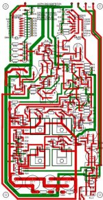
Layout drawing attached
Here's a sketch of the main board if anyone cares to comment.
I apologize for the fuzziness. This was the only way to keep the file size
under limit. I don't have a web site unfortunately. Feel free to email
me if you would like a better copy.
The board is for one channel MC and MM circuits. Muting circuit and power
supplies are not shown. I've added a draft of the inverting circuit to this
cut. Actual size is ca. 11.5 x 22 cm.
The layout roughly follows the service manual, with traces and final parts
placements improvised. A laundry list of departures from the schematic
is given below.
My biggest question is if the ground scheme is OK, but any help is welcome.
The ground starts off as the fat green trace at the bottom of the board.
Solder side is red. Component side is green.
I will be making my own boards and am not betting on anything until it's built
and tested, but it's been a good learning experience so far.
Boring details:
C7, 9,10 shown as electrolytic/polypropylene pairs, this could change
C7B bypass added
C7 optional shorting jumper marked, I expect to omit C7
C9B bypass added
C9 optional shorting jumper marked (I'm an optimist)
C10B bypass added
C38 omitted, this could change
R61 @ Q20 renamed R58
Q21-right renamed Q22
R28 @ C7 renamed R10
C12, 20 doubled and values increased (C12B,C20B added)
R4B trimpot added (thanks P. Daniels)
CB3 renamed CB1
CB4 renamed CB2
C? renamed C49
C29 @ Q10 renamed C25
C4,5 profiles shown for Panasonic polypropylene or possibly RelCap RTE polystyrene
C6 profiles shown for Panasonic polypropylene or possibly RelCap TFT teflon (axial)
C11 is silver mica since I can't find anything else
The isolating outlines around MOSFETs are sized for small heat sinks if needed.
Output traces are shown on the right side of the board. Plan B calls for shielded
coax.
I expect to add ground planes, which should be fun to try to get right.
Electrolytic caps are Panasonic NHG or TS for large values, coupling caps may
get upgraded to Black Gates
Film caps are Panasonic P-series polypropylene where possible
Resistors are Vishay/Dale RN60 except for R8,R9 which have oddball values,
these are Holco
Transistors are standard from MCM Electronics, except IRF9610 and ZTX450
are from DigiKey
Attachments
Congratulation, great work! I did some modification as well, C7/C9 are big MKPs (C38 is still a MKT), C41 is a 220uF electrolyte bypassed with 47nF MKP, C1 has now 1000uF (C41 has gone), C12/C20 are bypassed with 150nF MKTs… You don’t need heat sinks on the MOSFETs, they are pretty cold. As far as I can tell you, the ground plane is needed, I had some RF without them. Yeah, if you like, send me a better copy of your layout.
- Status
- This old topic is closed. If you want to reopen this topic, contact a moderator using the "Report Post" button.