Hi Cheff,
I have a couple of questions about your V3 circuit:
1) Why did you use a 1K load resistor on the output instead of a higher value? With 7ma of bias on the output transistors and a +-17V swing it seems like the transistors would be a bit starved for current at full swing. What did your simulation say? Did you use the low resistor value to reduce the absolute DC offset? With your load in parallel with the 1K resistor the total load will be even worse. Did you simulate the total load?
2) What did you find was the range of adjustment (in mv) with each of the two pots?
Thank you.
Graeme
gl said:Hi Cheff,
I have a couple of questions about your V3 circuit:
1) Why did you use a 1K load resistor on the output instead of a higher value? With 7ma of bias on the output transistors and a +-17V swing it seems like the transistors would be a bit starved for current at full swing. What did your simulation say? Did you use the low resistor value to reduce the absolute DC offset? With your load in parallel with the 1K resistor the total load will be even worse. Did you simulate the total load?
2) What did you find was the range of adjustment (in mv) with each of the two pots?
Thank you.
Graeme
Hi Graeme
OK, that's a real couple
") Your last couple was a couple of couple
Your last couple was a couple of couple Well, I had to make a compromise here again, since the output
impedance depends on this value (roughly Rout/2). A higher value
leads to a higher Zout, which I found to be undesirable for a preamp.
But Rout also affects the open loop gain, which increases as Rout
increases.
With a 10K pot at output, it doesn't affect Zout that much, so total
load won't have a great influence.
Rout also helps stabilizing the output offset, providing a reference
to ground to the collectors junction when the outputs are unloaded
(no pot), and a higher value would have increase the offset
instability as it amplifies any difference between the collectors
currents (Rout x Idiff)
So it's all about compromises, but my main concern was to keep a
relatively low Zout. And luckily, this value seems to have more
advantages than drawbacks
For the offset range, I haven't paid much attention to the limit
values, but my bad memory seems to say something like +/-20mV
for both... But I may be wrong here, so I'll try to check...
Oh my god... I'll have to detune this fabulous offset I've been
hunting for so long ...

Regards
Progress
Hello Cheff - thank you for your reply.
It was, in fact, your suggestion to consider transistors, other than the Zetex, that saved me. My ICAPs models for the Zetex must have been corrupt or highly incorrect (inappropriately applied?). When I replaced the models with Linear BC550/560 part models, which I downloaded from their website, the circuit suddenly sprung to life and simulations now make sense. I have just a couple questions for you:
1) Do you have any suggestions for designing for a SE input to SE out? I believe reducing the Rout to 500-ohms will help in that case, but the output swing is reduced by 1/2 (1/4 of balanced swing). Also, I simulate a slight differential offset when the negative input is grounded for SE operation. Any ideas how to add options to improve the output swing and/or diff offset in SE operation?
2) I’m curious why you chose to use the level-shifter current-mirror for output stage and not a FET, like in many other designs. Isn’t the linearity of the FET better when well biased? Did you get a chance to test the different emitter resistor values?
3) I simulated a 0.063% THD at 1K. Seems a bit high. Is that about you’re your sims showed? I know you measured quite a bit lower with the soundcard.
4) What are you using for PS? Why no local capacitors on the preamp boards? How about a LP filter on the input supplies?
5) Would gate-stoppers be prudent on the JFETs (~100-ohms)? I’m not sure they’re needed for RF on JFETs, but I’ve seen them used.
6) What are you using for volume control at the output? Did you say 10K pot? I was thinking a vol ladder, something like the twisted-pair JT.
7) Do you have a .pdf layout available for the V3 design yet?
Sorry for the seven x’s seven questions. Anything you can provide will help.
Thanks, Willus
Attachments
Re: Progress
Glad you have it working
The couple's now seven Everyday's inflation
I don't understand what you mean by SE in/out. Do you mean
Balanced/Unbalanced (sorry, english is not my native language...
Nobody's perfect) And why would you like to reduce Rout ?
The offset you simulate in unbalanced mode, is it a static or
dynamic one ?
I got no static offset when grounding one input in my sims.
And if I plot (V(out+)+V(out-)) in transient analysis (one input
grouded), I get for example a 25mV pp signal with a 6.5V pp.
Is it what you call an offset ?
I have chosen the current mirrors on an audio basis. For me, it was
far better than mosfets. Mosfet biasing was thermally limited by the
E-line package dissipation capabilities, but mostly by the offset
unstability when the mosfets were too hot. But you're welcome to try
And I will test different emitter resistor values, but give me one
week or two to listen to music
Mine gives 0.008% @ 1K, but I do not trust my simulator. Nor my
soundcard But it gives an idea...
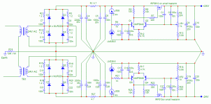
The PS is inspired from the Pearl's supply (see attached file)
There's no local caps, but the supply's output caps are close to the module :
The supply's on the right of the module (old ones ). And I didn't
feel the need for additional caps, nor of an additionnal ps filter.
Well, I didn't have problems with oscillations due to the lack of gate
resistors. But I have very short tracks on the pcb, so it may help.
But feel free to use some if you think it's more prudent. Or add a
ferrite bead on each gate lead before soldering the fets.
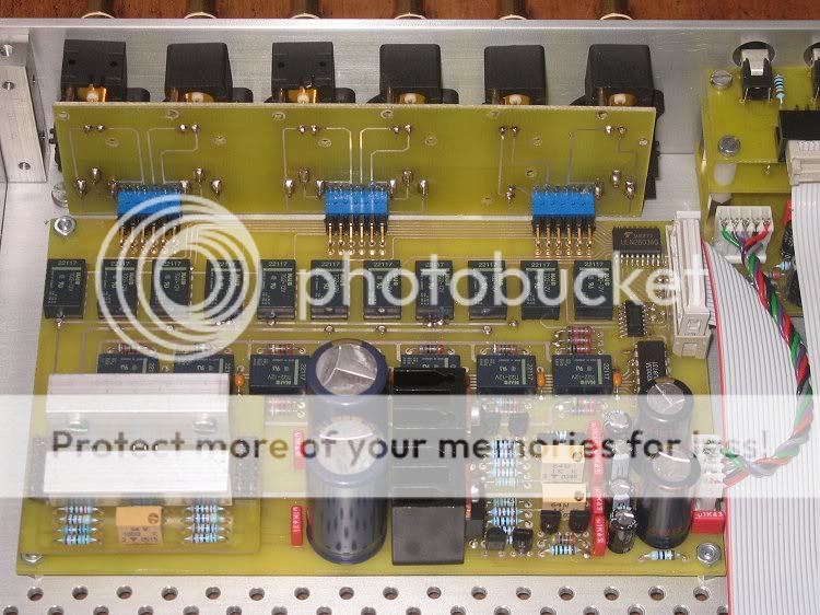
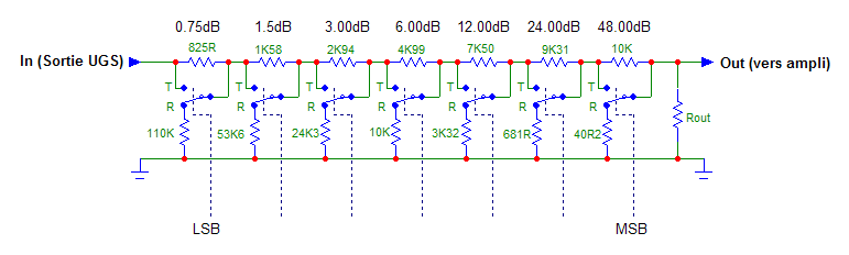
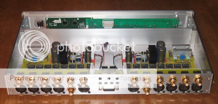
I use a balanced relay-based volume control (see the photo above -
it is hidden by the supply and the module), with a constant input
impedance of 10K :
Errr, what's a JT ?
See next post
You're welcome
z_willus_d said:Hello Cheff - thank you for your reply.
It was, in fact, your suggestion to consider transistors, other than the Zetex, that saved me. My ICAPs models for the Zetex must have been corrupt or highly incorrect (inappropriately applied?). When I replaced the models with Linear BC550/560 part models, which I downloaded from their website, the circuit suddenly sprung to life and simulations now make sense.
Glad you have it working
I have just a couple questions for you:
The couple's now seven
Everyday's inflation 1) Do you have any suggestions for designing for a SE input to SE out? I believe reducing the Rout to 500-ohms will help in that case, but the output swing is reduced by 1/2 (1/4 of balanced swing). Also, I simulate a slight differential offset when the negative input is grounded for SE operation. Any ideas how to add options to improve the output swing and/or diff offset in SE operation?
I don't understand what you mean by SE in/out. Do you mean
Balanced/Unbalanced (sorry, english is not my native language...
Nobody's perfect) And why would you like to reduce Rout ?
The offset you simulate in unbalanced mode, is it a static or
dynamic one ?
I got no static offset when grounding one input in my sims.
And if I plot (V(out+)+V(out-)) in transient analysis (one input
grouded), I get for example a 25mV pp signal with a 6.5V pp.
Is it what you call an offset ?
2) I’m curious why you chose to use the level-shifter current-mirror for output stage and not a FET, like in many other designs. Isn’t the linearity of the FET better when well biased? Did you get a chance to test the different emitter resistor values?
I have chosen the current mirrors on an audio basis. For me, it was
far better than mosfets. Mosfet biasing was thermally limited by the
E-line package dissipation capabilities, but mostly by the offset
unstability when the mosfets were too hot. But you're welcome to try
And I will test different emitter resistor values, but give me one
week or two to listen to music
3) I simulated a 0.063% THD at 1K. Seems a bit high. Is that about you’re your sims showed? I know you measured quite a bit lower with the soundcard.
Mine gives 0.008% @ 1K, but I do not trust my simulator. Nor my
soundcard
But it gives an idea...4) What are you using for PS? Why no local capacitors on the preamp boards? How about a LP filter on the input supplies?
The PS is inspired from the Pearl's supply (see attached file)
There's no local caps, but the supply's output caps are close to the module :
The supply's on the right of the module (old ones
). And I didn'tfeel the need for additional caps, nor of an additionnal ps filter.
5) Would gate-stoppers be prudent on the JFETs (~100-ohms)? I’m not sure they’re needed for RF on JFETs, but I’ve seen them used.
Well, I didn't have problems with oscillations due to the lack of gate
resistors. But I have very short tracks on the pcb, so it may help.
But feel free to use some if you think it's more prudent. Or add a
ferrite bead on each gate lead before soldering the fets.
6) What are you using for volume control at the output? Did you say 10K pot? I was thinking a vol ladder, something like the twisted-pair JT.
I use a balanced relay-based volume control (see the photo above -
it is hidden by the supply and the module), with a constant input
impedance of 10K :
Errr, what's a JT ?
7) Do you have a .pdf layout available for the V3 design yet?
See next post
Sorry for the seven x’s seven questions. Anything you can provide will help.
You're welcome
Attachments
So here is the pdf file for the pcb.
UGS V3 PCB
Sorry, but it's double-sided Take care of the scale when printing it, the actual module dimensions are given on page 2, along with the stuffing guide.
These are mirrored pcbs, so be careful before going U.V.
I added room for some compensation caps (CFB) if you happen to see some overshoot on square signals. Just in case, as I didn't find them necessary on my version...
Enjoy.
UGS V3 PCB
Sorry, but it's double-sided
Take care of the scale when printing it, the actual module dimensions are given on page 2, along with the stuffing guide.These are mirrored pcbs, so be careful before going U.V.
I added room for some compensation caps (CFB) if you happen to see some overshoot on square signals. Just in case, as I didn't find them necessary on my version...
Enjoy.
Cheff,
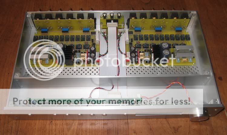
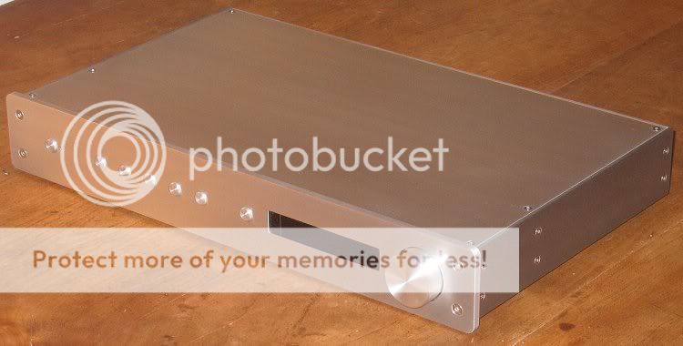
Congratulation on your very well implemented circuit. You make me want to upgrade from my X-BoSoZ. That last photo is a doozy, you spent a great deal of effort on integrating your circuitry together, and I'm impressed and jealous! Care to post a few more?!?
Cheers,
Terry
Congratulation on your very well implemented circuit. You make me want to upgrade from my X-BoSoZ. That last photo is a doozy, you spent a great deal of effort on integrating your circuitry together, and I'm impressed and jealous! Care to post a few more?!?
Cheers,
Terry
Banned
Joined 2002
metalman said:Cheff,
Congratulation on your very well implemented circuit. You make me want to upgrade from my X-BoSoZ. That last photo is a doozy, you spent a great deal of effort on integrating your circuitry together, and I'm impressed and jealous! Care to post a few more?!?
Cheers,
Terry
I agree maybe we can get a few made. ID like one.. Looks nice totally. Clean and straight forwared AND well layed out in order.


CheffDeGaar said:But do not forget the important things here are the little heatsinked stamps
Regards,
Definifly, big fingers are forbbiden here.....
I would say too : little stamps but maximum sound......Marc
Nelson Pass said:Cheff, are you available for adoption?
no-it's not ;
I was faster -he will adopt me
(what's better than be a spoiled child)
hehe,but -on second thought - having GrandPa with so much toys ......

Just to replace the Guy.......remembers Cheff's littles AX mono Blocs
As you can see his PassLabs addiction is during quite a long time.
Marc
An externally hosted image should be here but it was not working when we last tested it.
An externally hosted image should be here but it was not working when we last tested it.
An externally hosted image should be here but it was not working when we last tested it.
An externally hosted image should be here but it was not working when we last tested it.
As you can see his PassLabs addiction is during quite a long time.
Marc
Nelson Pass said:Cheff, are you available for adoption?
Wow !
Becoming the "Son of Zen" !!
Send the papers ! Thanks for the hommage... Really and deeply moved

CheffDeGaar said:Becoming the "Son of Zen"
Cheff,
don't kid yourself: You're French, he's after your wine stash !
(On the other hand, i've always wanted to be a PetitCheff)
Mmm, i see one of those nice GroupyB's arising.

- Home
- Amplifiers
- Pass Labs
- UGS adventures