every time i built new amp I having more or less trouble. nightmare with ZEN v4 and pretty fine with alephs. but more or less always was some bug. not this time I thought - all resistors was carefuly measured, all transistors was carefuly matched, soldered in triple checking BCE pins of bc550 and so on.. proud moove- power on- and no LIFE  all 10 boards. even no fire
rails are 25v after filtering. CSS mosfets SD and DG reads 7v or so, gain mosfets reads SD or DG 44V one irfp 9610 is sligty warming, 100ohm resistors are hot like a hell and 0,39ohm resistors shows no voltage across them. output reads -2,6V, speakers making small hum.
where is problem? all 3 trimers I tried from zero ohm to resitance half of what threy are (50K -set up to 25kogm and 200ohm to 100ohm)

all 10 boards. even no fire rails are 25v after filtering. CSS mosfets SD and DG reads 7v or so, gain mosfets reads SD or DG 44V one irfp 9610 is sligty warming, 100ohm resistors are hot like a hell and 0,39ohm resistors shows no voltage across them. output reads -2,6V, speakers making small hum.
where is problem? all 3 trimers I tried from zero ohm to resitance half of what threy are (50K -set up to 25kogm and 200ohm to 100ohm)
???
Where do we start?
Maybe you can state (link?) which schematic, pcb, ps you used.
Then you can state what measurements you took.
Why O why did you hook up all 10 boards?
Even after you saw the first one not working the way you
expected?
Part of the fun, should be fixing the circuit, if it's not working
the way it should.
Sigh...
I am a doctor,not electronic engineer. if one pacients is gone I trie to recover others jokes to jokes but its no funny. FETS are OK I think, resistors are ok. any problem I can imagine is bc550 transitors ,or input devices irf 9610..
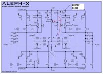
pcb boards is kristijan boards(2 originals and 8 cloned,but all of them did not work incl.originals). here is shematic-
http://www.kk-pcb.com/alephx.html
BTW thanks for help,I noticed throught 3 years beeing here is very friendly and helpfull people.
jokes to jokes but its no funny. FETS are OK I think, resistors are ok. any problem I can imagine is bc550 transitors ,or input devices irf 9610.. pcb boards is kristijan boards(2 originals and 8 cloned,but all of them did not work incl.originals). here is shematic-
http://www.kk-pcb.com/alephx.html
BTW thanks for help,I noticed throught 3 years beeing here is very friendly and helpfull people.
Her goes nothing
First problem i can think off at this moment (given the little info
to work with) is a problem around the current source above
the diff pair.
Did you check proper mounting and orientation of the 9.1V zener?
Kristian's schematic does not have reference designators
(i.e. zener is D1, Z1 or Dxxxx), but it's the only zener.
Use only one PCB to start testing, please!
Make sure your Powersupply is working properly, before any
testing!
All measurement referenced to ground:
Measurement 1
Measure the + rail (suppose +22 Volt)
Measurement 2
Measure the voltage at the node connecting the zener, the 4k7
resistor to ground, and the 221 gate resistor.
(see the problem when no ref.des.)
This voltage should be 22V - 9V = +13V
Please report back.
hi rtirion,
luckily today I had enought brains to leave all this for tomorow morning and go home from my speakers building workshop. \
will measure tomorow. I checked zenner. this marked side goes to pcb marked side and arrow goes to 22V.
power suply is OK. has no CLC filtering, also I am trying to start one channel so I conect only half caps 28x 7100uf 40V but its no matter.
rails is 25V not 22V but its OK?
second measurement is this way?
Attachments
25 V is OK
25V-9V = +16V on the positive zener lead.
Your diagram shows 2 red lines to two different points. Not good!
If the red line is your meter's plus probe it should only
measure the positive (unmarked) lead of the zener.
If the blue line is your meter's minus probe, it should be
connected to ground at all times during your measurements.
Choose appropriate voltage range on measurement instrument.
If this measurement is OK (around 16V) we will discuss
measurent 3 tommorow.
some measured values
Hi, unfortunately there was correct values- 16,1V
here is some measured values maybe this helps-
Reference to ground(one mulrimeter end connected to zero potential power supply lead and other at targeting point)
Most measurements are identical in both balanced sides of pcb
Gain mosfets Gate 25,7, Drain 20,8 Source 26,5
CSS mosfets 25,3 25,3 21,4
irf9610 (both) 20,5 25,5 24,1
irf 9610 (single) 16, 24,1 24,1
BC 550c transistors
(Pair near 220uf electrolytic in schematic) E 21,2 B 21 C 25,1
(other pair) 26 26,1 25,5
values measured at transistors-
Gain mosfets GD 46,8 DS 47,5 GS 0,5
CSS mosfets 0 4,2 4,1
Irf9610 (pair) GD 46,8 DS 49,5 GS 3,4
Irf9610 single 8,1 0 8
BC550
(closer to electrolytic in shemetic) EB 0,18 BC 4,13 EC 4,3
(other pair) 0 0,5 0,5
across resistors ) 0,39ohm 0volts
3x100ohms- 20,6V
3x100ohms resistors get very hot.
And 3 resitors 0,39ohms which one leg goes to to GAIN mosfets to Source pin(S) are little warm , and in one balanced side(-) looks like one 0,39ohm which goes to CSS mosfet to Source pin are little warm. Others lef 0,39ohm resistors to css and all other 5w resistors are cold.
>3x100ohms resistors get very hot.
No suprise. The outputs with reference to ground sit at the rail.
>Hi, unfortunately there was correct values- 16,1V
Do you mean -16,1V? I doubt that. Could that be +16,1V?
>Gain mosfets Gate 25,7, Drain 20,8 Source 26,5
>CSS mosfets 25,3 25,3 21,4
Also not good. The lower IRFP240 (your ref gain mosfets?)
should show negative voltages.
Maybe you could correct your post with proper signs before
each voltage.
Being meticulous and precise when measuring is very important.
Writing down the correct values, including the sign, is the only
way to go.
Otherwise it will be very difficult to help.
Maybe you can specify the rails?
+26,5 and -26,5 V (ref to ground)?
here is updated signs , where can be problem?
Hi, unfortunately there was correct values- +16,1V
here is some measured values maybe this helps-
Reference to ground(one mulrimeter end connected to zero potential power supply lead and other at targeting point)
Most measurements are identical in both balanced sides of pcb
Gain mosfets Gate +25,7, Drain +20,8 Source +26,5
CSS mosfets +25,3 +25,3 +21,4
irf9610 (both) +20,5 +25,5 +24,1
irf 9610 (single) +16, +24,1 +24,1
BC 550c transistors
(Pair near 220uf electrolytic in schematic) E +21,2 B +21 C +25,1
(other pair) +26 +26,1 +25,5
values measured at transistors-
Gain mosfets GD +46,8 DS +47,5 GS +0,5
CSS mosfets 0V +4,2 +4,1
Irf9610 (pair) GD +46,8 DS +49,5 GS +3,4
Irf9610 single +8,1 0V +8
BC550
(closer to electrolytic in shemetic) EB +0,18 BC +4,13 EC +4,3
(other pair) 0V +0,5 +0,5
across resistors ) 0,39ohm 0volts
3x100ohms- +20,6V
That does not help :-(
Where is the measured rails?
You should have +26V on the postive rail.
And -26V on negative rail.
This when you connect the black measurement lead to ground.
red measurement leadto a targeting point.
You fail to specify the rails? Why? (Asked in post
Is there no negative voltage in your circuit?
Then what does your powersupply look like?
What schematic did you use for the powersupply?
Seems I am repeating my self. And based on the second set of
measurments there is a serious powersupply mistake. And or
misplacement of the ground
I just had a look at kristijan's PCB.
see kristjian's pcb
I was unable to locate a ground connection,
other than the input grounds.
If your input connector is isolated, this input-ground (and
circuit ground) will never be connected to the powersupply,
hence no negative voltages, and the circuit will not function
properly.
Do you have a groundwire running from the amplifier PCB
to your powersupply ground?
My previous post crossed yours. Sorry about that
in this picture you give link is small area of 4 inputs. and one of theese(actualy two,but second one is for line input ground) called GND to this gnd I conected my zero potential ground(one cap plius is plus,then the same cap minus conected with other caps plus and here we have zero potential)and the last pin minus is minus to PS I conected this zero potential to gnd NOTE that I did folowing power suply with 2 bridges(both secondaries goes to bridge AC legs ,and from one bridge I take plus, the same bridge minus conected to another bridge plus and have zero potential, and last pin is minus whee it minus of PS
Based on your previous description the powersupply seems OK
But the measurements don't show any negative voltages.
Howcome?
Measurement 3
If you measure the -PWR on the amplfier board,
so red probe on -PWR and black probe on GND,
you should see -26,5V.
Is this the value you see?
Measurement 4
With black probe on ground:
Measuring on the gate off the "gain transistor"
shows "Gate +25,7" but it should be around -20V
can you confirm this?
Based on your previous description the powersupply seems OK
But the measurements don't show any negative voltages.
Howcome?
Measurement 3
If you measure the -PWR on the amplfier board,
so red probe on -PWR and black probe on GND,
you should see -26,5V.
Is this the value you see? Yes Sorry its MINUS 26,3 not plus
Measurement 4
With black probe on ground:
Measuring on the gate off the "gain transistor"
shows "Gate +25,7" but it should be around -20V YES ITS MINUS SORRY AGAIN. i ENTER WRONG VALUES ,I WILL MEASURE NOW CAREFULLY AGAIN ALL AND WRITE BACK
can you confirm this?
HERE IS CORRECT VOLTAGEs.
here is some measured values maybe this helps-
Reference to ground(one mulrimeter end connected to zero potential power supply lead and other at targeting point)
Most measurements are identical in both balanced sides of pcb
Gain mosfets Gate -25,7, Drain +20,8 Source -26,5
CSS mosfets +25,3 +25,3 +21,4
irf9610 (both) +20,5 -25,5 +24,1
irf 9610 (single) +16, +24,1 +24,1
values measured at transistors-
Gain mosfets GD +46,8 DS -47,5 GS -0,5
CSS mosfets-0V(??) -4,2 -4,1
Irf9610 (pair) GD +46,8 DS -49,5 GS -3,4
Irf9610 single +8,1 0V +8
Given +PWR = 26,5V and -PWR = -26,5V
Measurements ground referenced
>Gain mosfets Gate -25,7, Drain +20,8 Source -26,5
That's not good. Should be around:
Gate -21V, Drain 0V, Source -26V. In this case your source resistor
would be dropping |0,5V|.
>CSS mosfets +25,3 +25,3 +21,4
That's also not good. Should be around:
Gate +4,5V, Drain +26,5V (rail), Source +0,5V
>irf 9610 (single) +16, +24,1 +24,1
Also not good. Should be around:
Gate +16V, Drain +4V, Source +20V
Way off, as you can see.
>BC 550c transistors
>(Pair near 220uf electrolytic in schematic) E +21,2 B +21 C +25,1
No good. Should be around
E = 0V, B = 0,7V, C = 4,5V
There have been a lot of problems around these BC550C.
Given these measurements, this would be my prime suspect.
What brand did you use? Do you have the datasheet from the
manufacturer? Check the orientation again? Do not let the
markings on the PCB silkscreen, determine the correct position.
There are two types of bc550. Leads inline and Leads in triangle.
Pinning CBE for type one EBC type two. Which one do you have?
Fairchild, Zetex, Philips, Siemens? Allocate the proper sheet and
determine the correct lead out. Cross check with board pads.
Use a simple transistor meter to get an indication of gain
BC550C should have a hfe of 400 - 800. This way you know
which leg is C, B and E
The measurments on the diffpair are inconslusive.
two parts with exactly the same figures for G, D and S.
Not possible. Sources are connected, so they give same reading.
Drains should differ a little bit. Same goes for the gates.
Please repeat measurements around these.
bc550 transistors are conected right way(I think) because I mached them to pairs with digital multimeter hfe function to mach. this function wouldnt work if i do not conect to right pins.
is it posibly problem in some resistors? could it be that resitors from same tape can be diferent,lets say 4,7kohm and accidently 47kohm, because I did not measure all resistors.
the firs thing waht i will do tomorow is recheck all resistors, I am 100%sure that mosfets gain and css conected OK,and 90%posibility that bc550c conected ok mine is all legs in line,probbaly from philips or siemens, did not searched for irf9610 pins but its is the same as in irfp240. just soldered in places where threy belong.
what a headache..
- Status
- This old topic is closed. If you want to reopen this topic, contact a moderator using the "Report Post" button.
- Home
- Amplifiers
- Pass Labs
- 10 pieces aleph x and non of theese working