This question is directed towards anyone and everyone, Mr. Pass included.
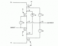
Attached is the modulated supply picture.
==> If I understand correctly, the positive voltage swing of the output would be about (V++) - 27V (if the output voltage goes any higher, the drain of the upper cascode would hit the voltage rail).
Similarly, the lower output voltage swing would be (V--) + 29V.
Just as a suggestion for improvement:
Eliminate the 27V and 29V sources, and replace them with a resistor divider between the output and the upper rail for the 27V source, and the output and the lower rail for the 29V source, to control the gates of the cascode transistors. Both resistor dividers would have two equal resistors with the midpoint connected to the gate of the respective cascode transistor.
In this way, the voltage difference from V++ to the output is placed on the two NFETs equally, and the voltage difference between the output and V-- is distributed between the two PFETs equally. This would allow a higher voltage swing overall. I know that we are trying tog et the voltage across the inner FETs low (to keep power consumption down).
Attachments
If you go to this site you will find several articles by Nelson Pass. There is one on "Cascoded amplifier design" that outlines what are the advantages of a fixed voltage vs one proportional to the signal across a given transistor. This article helps explain why a resistor divider will have quite a different effect than the fixed offset scheme.
http://www.passlabs.com/articles.htm
Cascoded designs have been around for a long time and like many other designs the devil is in the details. Still, they offer one solution to transistor distortion, so understanding why they work is very useful.
http://www.passlabs.com/articles.htm
Cascoded designs have been around for a long time and like many other designs the devil is in the details. Still, they offer one solution to transistor distortion, so understanding why they work is very useful.
"27" and "29" are simply labels for voltage sources. It's normal practice for a patent to use numeric labels like that. There is no limitation on the construction of the voltage source; resistors are fair game. In fact, thats almost certainly the method Nelson used, himself (in practice, probably a pot). However, specifying a voltage source in the generic sense allows for things like regulated voltages or perhaps even modulated voltages.
Note that the voltages at 27 and 29 will almost certainly be different due to the real world differences in Vgs between 17 and 19. Thus, it's conceivable that the voltages at 27 and 29 might coincidentally turn out to be 27 and 29V. Don't bet the farm on it, though.
Something to think about...what if you were to replace 11 and 13 with JFETs?
Grey
rtarbell said:(edit....)
Just as a suggestion for improvement:
Eliminate the 27V and 29V sources, and replace them with a resistor divider between the output and the upper rail for the 27V source, and the output and the lower rail for the 29V source, to control the gates of the cascode transistors. Both resistor dividers would have two equal resistors with the midpoint connected to the gate of the respective cascode transistor.
In this way, the voltage difference from V++ to the output is placed on the two NFETs equally, and the voltage difference between the output and V-- is distributed between the two PFETs equally. This would allow a higher voltage swing overall. I know that we are trying tog et the voltage across the inner FETs low (to keep power consumption down).
Originally posted by djk
That's not what the patent is about.
I was replying to the thread starter, rtarbell, not to the patent. The poster recommends making the outside transistor pair follow 1/2 the output voltage swing. While this does distribute the heat accross two pairs and does allow for larger swings, the patent drawing is of a cascode design. i.e. the Voltage accross the output drive transistor is constant with output voltage swing.
By replacing the voltage sources 27 and 29 with a resitor divider the benefits of a cascode design are lost. It is a different circuit topology and while either topology can be made to work well, rtarbell's "suggestion for improvement" seems to have missed the point.
"Voltage accross the output drive transistor is constant with output voltage swing."
Items 11 and 13 are the outputs. The supply for them is from item 33, a CCS. It looks like the voltage across 11 and 13 does not become constant until item 33 runs out of current and it comes through items 17 and 19, at this point items 11 and 13 are cascoded by items 17 and 19.
A clever variation on class G.
Did Nelson Pass ever make a commercial version of this?
djk said:"Voltage accross the output drive transistor is constant with output voltage swing."
Items 11 and 13 are the outputs. The supply for them is from item 33, a CCS. It looks like the voltage across 11 and 13 does not become constant until item 33 runs out of current and it comes through items 17 and 19, at this point items 11 and 13 are cascoded by items 17 and 19.
A clever variation on class G.
Did Nelson Pass ever make a commercial version of this?
Item 33 is a constant current conductor (it does not supply power) The current for item 33 comes from items 17 and 19. Items 17 and 19 are source followers: i.e. the source voltage is equal to the voltage of item 27 or 29 minus VGs for each of the FETs. The voltage acrross Items 11 and 17 is indeed constant and in this design Item 33 only runs out of current during some fault condition.
Current source is something of a misnomer since they simply regulate the current supplied by some other circuit component. Current sources may appear to supply current from one leg, but it is the exact same current that is fed into them on the other. In the standard definition, current source only means that the current on each leg of the two legged device is identical and constant, assuming only that a sufficient source voltage is available.
Your current source is is not a two wire device although it is drawn as one. Guess it serves me right for not reading the body of your patent (still the current arrow should have warned me - oh well).
So having not read it, let me climb a little further out on that limb. Since the voltage across the two FETs items 11 and 13 is fixed and the bias is fixed by item 25, the current through 11 and 13 is also approximately constant (in lieu of signal).
So the current supplied by item 33 can only be part of the idle current in items 11 and 13 the rest presumably comes from FETs 17 and 19.
Engineers have wrestled with the problems created when of one half of a push-pull design goes to a zero current state as the output current changes polarity . The traditional solution has always been a class A amplifier which has the unfortunate side effect of generating prodigious amounts of heat and being quite inefficient. Lately many designs where the output supply voltage follows the waveform either linearly or in a stepwise fashion have become popular or the converse where the output bias follows the signal so the idle current stays above the required swing (I believe Krell does this).
I wrote the above because since you have made the output of your proposed design somewhat more complex than the minimum required. I'm guessing that the current source 33 isn't supposed to turn on and off during parts of the output waveform, is this correct?
Hopefully without revealing trade secrets, can you say what percentage of the output drive current comes from item 33 and from FETs 17 and 19?
Hi, Hermanv,
Part#33 is indeed a current source. A big one. You can see here
http://www.diyaudio.com/forums/attachment.php?s=&postid=335698&stamp=1077846709
#33 is Tanggo tranformer, 7A (yes, 7 ampere of it). So it is not part of bias supplied from main rail voltages, but independent low voltage-high current floating transformer.
With this patent you can pass very big bias current (Ampere magnitude, not mA), yet dissipate low heat (because of low voltage drop). This is the best part. The result is the output transistor (which connects to the speakers) works in their VERY LINEAR region. You cannot immitate such condition by making ErrorCorrection, for example, only raw current can make it.Engineers have wrestled with the problems created when of one half of a push-pull design goes to a zero current state as the output current changes polarity . The traditional solution has always been a class A amplifier which has the unfortunate side effect of generating prodigious amounts of heat and being quite inefficient.
If the music is low level, the current flowing to speaker maybe 100's of mA, but the steady current passing thru the output transistors are always 7A in this example. So the bias is much bigger than the output current in this low level example.Hopefully without revealing trade secrets, can you say what percentage of the output drive current comes from item 33 and from FETs 17 and 19?
- Status
- This old topic is closed. If you want to reopen this topic, contact a moderator using the "Report Post" button.
- Home
- Amplifiers
- Pass Labs
- The modulated supply and voltage swing (patent #5,343,166)