Hi,
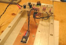
Finnaly I've manage to test atleast first half of my MiniA (L channel that is)")
So – my findings:
- well, it works (at least in mono arrangement )
- measured numbers are (the marks of elements are from A5 schematic in Service manual) :
o DC offset at output 28-30mV
o Voltage drop on R11 5,53V
o From Source of Q1 Q2 pair to gnd: 3,58V
o Q4 C-E: 4,94V
o Q5 C-E: 4,94V
o Z5: 9,2V (I guess my voltmeter ain't very precise)
o And on power source resistors in both cases 0,47V à so I guess bias is currently set to around 1A or maybe even a bit less (since my resistor is made out of 2 parallel 1R ones). My goal is to get around 1,3A of bias ..
o D-S voltages on irfp240 are 15,1V
o BUT there is something I wonder – I bought 9610 from a guy as allready matched pairs …
Now in working circuitry I've measured VGS of them: Q1 = 3,56V, Q2 =
3,59V (hmm – that's allready on the border of 30mV) and Q3 = 3,71V?!?!? (but this one draws a bit higher current and so VGS is higher, right?) Now I just wonder – the guy who sold them to me – matched them to 5,26V (in the case of these pair) – so I guess he did it at much higher current – but – and now my Qusetion:
is this current/VGS ratio linear or not? Does this difference of Q1 and Q2 means they are not well (I've got another 8 »matched« pairs of them waiting for my projects) matched at all or just not matched for my demands?
Thanks
Finnaly I've manage to test atleast first half of my MiniA (L channel that is)
So – my findings:
- well, it works (at least in mono arrangement
)- measured numbers are (the marks of elements are from A5 schematic in Service manual) :
o DC offset at output 28-30mV
o Voltage drop on R11 5,53V
o From Source of Q1 Q2 pair to gnd: 3,58V
o Q4 C-E: 4,94V
o Q5 C-E: 4,94V
o Z5: 9,2V (I guess my voltmeter ain't very precise)
o And on power source resistors in both cases 0,47V à so I guess bias is currently set to around 1A or maybe even a bit less (since my resistor is made out of 2 parallel 1R ones). My goal is to get around 1,3A of bias ..
o D-S voltages on irfp240 are 15,1V
o BUT there is something I wonder – I bought 9610 from a guy as allready matched pairs …
Now in working circuitry I've measured VGS of them: Q1 = 3,56V, Q2 =
3,59V (hmm – that's allready on the border of 30mV) and Q3 = 3,71V?!?!? (but this one draws a bit higher current and so VGS is higher, right?) Now I just wonder – the guy who sold them to me – matched them to 5,26V (in the case of these pair) – so I guess he did it at much higher current – but – and now my Qusetion:
is this current/VGS ratio linear or not? Does this difference of Q1 and Q2 means they are not well (I've got another 8 »matched« pairs of them waiting for my projects) matched at all or just not matched for my demands?
Thanks
Attachments
I have wondered the same thing and can only assume that a matched pair is NOT a matched pair unless matched at the same current as the situation. I have had the same results as you, stabist. I have resorted to matching them 'in situ'. I don't solder them in real good until I swap in ones that match...
Well now after first excitement at 4am is gone - I've readed articels abouut matching - and realized I'm right - if transistors are matched at such current that VGS is e.g. 5V - that doesn't mean they will be matched at the current with VGS 4V ...
Another way than yours mpmarino is simply add that additional resistor ...
BUT!! then again - how can I calculate enough precize value - because my DMV has got not enough digits to find out is it 25mV or 34mV difference ...
Btw - this resistor - it is put in series to source of the transistor with lower VGS - RIGHT??
- I've readed articels abouut matching - and realized I'm right - if transistors are matched at such current that VGS is e.g. 5V - that doesn't mean they will be matched at the current with VGS 4V ... Another way than yours mpmarino is simply add that additional resistor ...
BUT!! then again - how can I calculate enough precize value - because my DMV has got not enough digits to find out is it 25mV or 34mV difference ...
Btw - this resistor - it is put in series to source of the transistor with lower VGS - RIGHT??
Hi Primoz
I would consider power MOSFETs matched within 10mV Vgs a very good match (so 30mV is not so bad). Unlike FETs, bipolars are much easier to match so matching within 2 mV is usually not difficult to obtain.
Anyway all you need to measure Vgs (for matching purposes) is a DC source of about 9-12V, resistor and a voltmeter. To measure N-channel devices connect the source to 0V (GND), short the gate and drain and connect a resitor between the drain and + pole of the DC source (Vdd). At this point you measure MOSFET's Vgs that corresponds to the drain current (Vdd-Vgs)/R where R is the value of the used resistor (i.e. test Id is set by R). To test P-channel devices just swap the poles of the DC supply.
Chip
Btw - this resistor - it is put in series to source of the transistor with lower VGS - RIGHT??
Dunno.. I always thought it would be in parallel with the fet with the higher vgs, but I'm probably wrong.
I am pretty sure Nelson advertised that matching was done 'in situ' on the later alephs. Personally it works for me, and I have found that it is more accurate and takes less time. When you get a pair that has low offset...your done! Easy as pie and no tedious measurements or wondering. My 2 pennies.....
redards
mpmarino,
I have not really learn how to match transistors but your method sound easier. Can you write out a few bullet points of what you meant by "in situ" and the procedure of how you go about achieving it?
I think you meant by poping in/out the transistors by trial and error and measuring it and see which one(s) will get the closest match, to within 10mv. Questions like .... , which pin terminals to measure, etc ...?
fcel said:mpmarino,
I have not really learn how to match transistors but your method sound easier. Can you write out a few bullet points of what you meant by "in situ" and the procedure of how you go about achieving it?
I think you meant by poping in/out the transistors by trial and error and measuring it and see which one(s) will get the closest match, to within 10mv. Questions like .... , which pin terminals to measure, etc ...?
Yes, I did mean trial and error.. to a point (I guess you could go in circles for a while!). On the two alephs I have built (one a mini A, so the output fets being matches is irrelevant) I attempted using 'matched' 9610's only to find a little more DC offset at the output than I was happy with. I then simply focused on only 1 fet in the diff pair and kept swapping in a new fet until I was happy with the output DC offset. Maybe you would have to give up on that one and try swapping the other fet to make it balance. The fets I have are from the same lot and I started with quite a few, they were pretty close already. Seems to me you can have guaranteed good results if you have enough fets. Funny that the fets I ended up with in the amps were not matches from my 'matching session'. So much for my matching abilities!

Stabist comment about measuring VGS throw me first. What does it mean by measuring VGS? Is that the voltage between pin G and S?
To make sure that I understand you. You are saying ... pop the 9610 in and measure ONLY the output DC offset? No need to measure anything else?
We want to have output DC offset to be less than 10mV? 5mV?
To make sure that I understand you. You are saying ... pop the 9610 in and measure ONLY the output DC offset? No need to measure anything else?
We want to have output DC offset to be less than 10mV? 5mV?
@chip
Thanks - alltough I have to admit I know this circutry - it's just the thing I'm a bit pissed because I've bought like exactly matched pairs from this guy - but now it seems that doesn't be so ...
And OK, I can live with that from the aspect of 9610 - BUT - I also bought 14 matched 240 ones for my A30 - and now I have doubts they are matched well ... And in the case of output transistors - I'm a bit more worried ...(
Will have to test them myself I guess - so I just have to get some extra time ...
@fcel
Yep VGS is G-S voltage ...
I think that this method mentioned by mpmarino is also a bit slow - I think you must wait for each measurment again like 10, 15min - so everything settles down and the amp worms up and all ...
Thanks - alltough I have to admit I know this circutry - it's just the thing I'm a bit pissed because I've bought like exactly matched pairs from this guy - but now it seems that doesn't be so ...
And OK, I can live with that from the aspect of 9610 - BUT - I also bought 14 matched 240 ones for my A30 - and now I have doubts they are matched well ... And in the case of output transistors - I'm a bit more worried ...
( Will have to test them myself I guess - so I just have to get some extra time ...
@fcel
Yep VGS is G-S voltage ...
I think that this method mentioned by mpmarino is also a bit slow - I think you must wait for each measurment again like 10, 15min - so everything settles down and the amp worms up and all ...
fcel said:Stabist comment about measuring VGS throw me first. What does it mean by measuring VGS? Is that the voltage between pin G and S?
To make sure that I understand you. You are saying ... pop the 9610 in and measure ONLY the output DC offset? No need to measure anything else?
We want to have output DC offset to be less than 10mV? 5mV?
I feel like I've thrown stabist's thread off track and I apologise for that. This will be the last of my meddling.
Please understand me, I'm no expert and have very little experience with this circuit compared to some/most on this forum...just that I feel like I learn some by discussing things. Anything I say that's off I expect to get corrected, in fact I hope so!
Yes measuring vgs is simply turning the fet on by running current thru and measuring voltage gate to source. Nelson has a simple procedure somewhere on his passdiy site, and chip_mk described it a few posts ago.
I am saying that in my experience, vgs matching of the diff pair got things pretty darn close, but I still had maybe 20-30mv at the output (actually I guess that's OK but I wanted it better. I assume that unless every component(1/4 watt resistors around the 9610s..etc..etc) is perfectly matched you will have offset at the output. Finding the 'magic' pair worked for me. The way I understand it,the goal of matching the differential pair is to approach 0v offset. Please tell me if I'm an idiot

Stabist, your absolutely right. It is slow!
Hi,
mpmarino - don't stop posting here - it's OK!! Actually it has much to do with my MiniA!!!
Btw - changed some things - so now insted of 0R5 i have 0R33 Source resistors ... Also additional resistors added in output sense field ...
Result:
- around 1,4A of bias (that was my goal)
- but now the difference in the dif pair is going up - it's allread 40mV - and DC offset at the output is now jumping from 30-45mV!!!
SO - I'll do something else - I have some irfp9620 I've purchased about 2+ yrs ago and they were very very good matched at that time - and at such conditions my VGS was aroun 3,70V - that's like almost idela for my present demands
I'll change those 9610 for 9620 and see what will happen ...
mpmarino - don't stop posting here - it's OK!! Actually it has much to do with my MiniA!!!
Btw - changed some things - so now insted of 0R5 i have 0R33 Source resistors ... Also additional resistors added in output sense field ...
Result:
- around 1,4A of bias
(that was my goal)- but now the difference in the dif pair is going up - it's allread 40mV - and DC offset at the output is now jumping from 30-45mV!!!
SO - I'll do something else - I have some irfp9620 I've purchased about 2+ yrs ago and they were very very good matched at that time - and at such conditions my VGS was aroun 3,70V - that's like almost idela for my present demands
I'll change those 9610 for 9620 and see what will happen ...
Gee ....
Now I don't understand it at all ...
I've replaced 9610 with set of 9620 - they should be matched very well - because from same matching session some of them were allready taken for A5. And it works without any serious DC offset ...
Or is that just pure coincidence?? BECAUSE - now I've measured 150mV offset and also around 150mV of difference beetwen VgsQ1 and VgsQ2 ... ?!?!? Hmm ...
Please help - need confirmation
OK, so after around 5 different try outs I'm on around 45-50mV DC offset (that's 10+mV from the original pair - but didn't mark ie ) ...
Nevertheless - time to learn something:
(ALL MARKS are refering to original A5 schematic)
If I understand right - measuring voltage drop on R11 gives me 5,5V - so current to Q3 source is 5,5/221=24,8mA
Then R14 (392R) has 5,02V drop - so current is 12,8mA - that's a bit more than half of 24,8mA - and also in real life - Q1 has higher Vgs, etc ...
To compenzate that - I have to calculate a resistance to ADD TO Q2 - correct? If I understand correct - this resistor must be put in SERIAL to Source pin of Q2? Right??
OK, and to get value - total current is 24,8mA - so I want to achieve that Q1 and Q2 distribute this equaly - that is 12,4mA.
What I also know is VgsQ1= 3,60V and VgsQ2= 3,55V - so difference is around 50mV.
SO - I take 0,05V/0,0124A = 4R - and this is desirable resistance?? Right??
THANKS
OK, so after around 5 different try outs I'm on around 45-50mV DC offset (that's 10+mV from the original pair - but didn't mark ie
) ...Nevertheless - time to learn something:
(ALL MARKS are refering to original A5 schematic)
If I understand right - measuring voltage drop on R11 gives me 5,5V - so current to Q3 source is 5,5/221=24,8mA
Then R14 (392R) has 5,02V drop - so current is 12,8mA - that's a bit more than half of 24,8mA - and also in real life - Q1 has higher Vgs, etc ...
To compenzate that - I have to calculate a resistance to ADD TO Q2 - correct? If I understand correct - this resistor must be put in SERIAL to Source pin of Q2? Right??
OK, and to get value - total current is 24,8mA - so I want to achieve that Q1 and Q2 distribute this equaly - that is 12,4mA.
What I also know is VgsQ1= 3,60V and VgsQ2= 3,55V - so difference is around 50mV.
SO - I take 0,05V/0,0124A = 4R - and this is desirable resistance?? Right??
THANKS
Banned
Joined 2002
Re: Please help - need confirmation
Hi Stabist
Alephs are such design where the output DC offset depends on the input diff pair matching (like any other amplifier with diff pair at input) as well as the relation between the output MOSFET's Vgs and the the current source that supplies the input pair.
In terms of Aleph 5 it means this:
- At some voltage across R14 (let's name it Ve), Q18-Q20 bundle sinks as much current as Q6-Q8 generates. This is the equilibrium we are looking for.
- Voltage Ve present on R14 means that the current flowing through Q1's drain (let's name it I1) is I1=Ve/R14.
- On the other hand we would like to have balance between the currents flowing through Q1 and Q2 in order to minimize DC offset and to keep the pair polarized at the most linear part of the transfer curve.
- This balance can be acheived by choosing appropriate values for R11 and R14. The values given in the schematics are just approximation. Final result depends on the particular transistor Q3 and Z5 (as you know semiconductors have high spread of the parameters).
- Changing R14 would also affect the open loop gain and the frequency responce. The impact of R11 change is quiet neglectable to anything else except DC offset. Even you change the current flowing from Q3, I1 will remain essentially unchanged (in order to keep the output stage in equilibrium) but the rest goes through Q2.
In your case the disbalance is 0.8mA. Put an 6k8 resistor in paralel with R11. It will produce surplus of 5.5V/6k8=0.8mA flowing through Q3. This surplus will be absorbed completely by Q2 and the diff pair will be in balance. When the current through diff pair is balanced the output DC offset equals the difference in Vgs between Q1 and Q2 (i.e. how well matched they are).
I would not put anythig to Q2 as it would make input stage asymetric and generaly decrease the open loop gain of the amplifier.
In regard to MOSFETs matching, this is a quote from A2 service manual "We match the input devices to each other to within 0.2% and the output devices to within 2%." That means about 8mV for input devices (4V*0.2/100) and about 60mV for output devices (3V*2/100).
BTW Has your nickname something to do with Kuzma's Stabi/Stogi?
Pozdrav,
Chip
Stabist said:OK, so after around 5 different try outs I'm on around 45-50mV DC offset (that's 10+mV from the original pair - but didn't mark ie
Nevertheless - time to learn something:
(ALL MARKS are refering to original A5 schematic)
If I understand right - measuring voltage drop on R11 gives me 5,5V - so current to Q3 source is 5,5/221=24,8mA
Then R14 (392R) has 5,02V drop - so current is 12,8mA - that's a bit more than half of 24,8mA - and also in real life - Q1 has higher Vgs, etc ...
To compenzate that - I have to calculate a resistance to ADD TO Q2 - correct? If I understand correct - this resistor must be put in SERIAL to Source pin of Q2? Right??
OK, and to get value - total current is 24,8mA - so I want to achieve that Q1 and Q2 distribute this equaly - that is 12,4mA.
What I also know is VgsQ1= 3,60V and VgsQ2= 3,55V - so difference is around 50mV.
SO - I take 0,05V/0,0124A = 4R - and this is desirable resistance?? Right??
THANKS
Hi Stabist
Alephs are such design where the output DC offset depends on the input diff pair matching (like any other amplifier with diff pair at input) as well as the relation between the output MOSFET's Vgs and the the current source that supplies the input pair.
In terms of Aleph 5 it means this:
- At some voltage across R14 (let's name it Ve), Q18-Q20 bundle sinks as much current as Q6-Q8 generates. This is the equilibrium we are looking for.
- Voltage Ve present on R14 means that the current flowing through Q1's drain (let's name it I1) is I1=Ve/R14.
- On the other hand we would like to have balance between the currents flowing through Q1 and Q2 in order to minimize DC offset and to keep the pair polarized at the most linear part of the transfer curve.
- This balance can be acheived by choosing appropriate values for R11 and R14. The values given in the schematics are just approximation. Final result depends on the particular transistor Q3 and Z5 (as you know semiconductors have high spread of the parameters).
- Changing R14 would also affect the open loop gain and the frequency responce. The impact of R11 change is quiet neglectable to anything else except DC offset. Even you change the current flowing from Q3, I1 will remain essentially unchanged (in order to keep the output stage in equilibrium) but the rest goes through Q2.
In your case the disbalance is 0.8mA. Put an 6k8 resistor in paralel with R11. It will produce surplus of 5.5V/6k8=0.8mA flowing through Q3. This surplus will be absorbed completely by Q2 and the diff pair will be in balance. When the current through diff pair is balanced the output DC offset equals the difference in Vgs between Q1 and Q2 (i.e. how well matched they are).
I would not put anythig to Q2 as it would make input stage asymetric and generaly decrease the open loop gain of the amplifier.
In regard to MOSFETs matching, this is a quote from A2 service manual "We match the input devices to each other to within 0.2% and the output devices to within 2%." That means about 8mV for input devices (4V*0.2/100) and about 60mV for output devices (3V*2/100).
BTW Has your nickname something to do with Kuzma's Stabi/Stogi?
Pozdrav,
Chip
chip_mk, if I got your explanation right...Stabist can also either tune his Aleph DC offset by replacing R11 or R14 with a trimpot say 500ohms. He can either tune with R11 so as he can have double the current through R14 or he can tune R14 to have half of the total current through R11. He can best tune either way by monitoring DC offset at the output.
Sorry to do a promotion here but the HotRod Aleph Boards feature this tuning setup...to borrow NP:
Sorry to do a promotion here but the HotRod Aleph Boards feature this tuning setup...to borrow NP:
- Status
- This old topic is closed. If you want to reopen this topic, contact a moderator using the "Report Post" button.
- Home
- Amplifiers
- Pass Labs
- 1 channel of MiniA working - measurments