This is a SOZ transconductance amp I began building last Aug/Sept. and first turned on about Feb. 1. It's primary goal was to be a learning experience on current amps. For the most part this is an embodiment of all the "crumby hints" dropped by NP on this site as well as the good stuff included in the Zen articles. For my part there has been a great deal of cut-and-try experimentation and attendant headscratching. The amp was first turned on at beginning of February. At this point it plays music quite well although there is still a bit more distortion present than I think should be there.
There has been a relatively small and diminishing amount of interest in transconductaance amplifiers on this site over the last 8 months but that seems to have changed suddenly. For that reason I have decided to post this project such as it is.
This is not a copy of the F1. It was designed to use existing junk box parts. The heat sinks for instance are old Ampex TBC-1 sinks and the transformer is a Signal 88-8 from a long-gone A40. The sinks weren't up to F1 levels of heat dissipation so the CCS's were dropped from 1.75 amps to 1.4. This let me use .47 ohm 3W resistors, which I had on hand, to set the current. The 1.4 amps meant I could use single resistors in the places where NP had to parallel two parts in the F1. It all worked out quite nicely. I figure I'm getting about 6 to 8 watts - more than enough.
I currently use this piece with a pair of Fe166E's on quick and dirty MDF open baffles. By my calculations it produces approximately 15dB of gain with an 8 ohm load. I drive it from a single ended source and so lose 6dB. Even with 9dB of net gain into a high efficiency driver the gain does not seem as high as I would have expected.
If NP was not going to publish the F1 service manual shortly then I would keep on experimenting. I have a definite list of things to try. As it is I am going to stop work and wait for the F1 details to emerge. This has been a fun project. And although I don't consider it to good enough to rate stickers it has certainly met its goal of teaching me a lot about transconductance power amps.
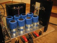
The photo is fuzzy because the shiny metal confused the camera autofocus. It's a good thing because this partially obscures the electronic hairball on the perf board. The two visible transistors at the top of the right heatsink are the SFH9240 CCS's.
Thanks everyone for their encouragement - you know who you are - and NP in particular for the "crumbs" and the support. If there is sufficient interest I would be happy to clean up and post the schematic with more details about the circuit.
Best Regards,
Graeme
There has been a relatively small and diminishing amount of interest in transconductaance amplifiers on this site over the last 8 months but that seems to have changed suddenly. For that reason I have decided to post this project such as it is.
This is not a copy of the F1. It was designed to use existing junk box parts. The heat sinks for instance are old Ampex TBC-1 sinks and the transformer is a Signal 88-8 from a long-gone A40. The sinks weren't up to F1 levels of heat dissipation so the CCS's were dropped from 1.75 amps to 1.4. This let me use .47 ohm 3W resistors, which I had on hand, to set the current. The 1.4 amps meant I could use single resistors in the places where NP had to parallel two parts in the F1. It all worked out quite nicely. I figure I'm getting about 6 to 8 watts - more than enough.
I currently use this piece with a pair of Fe166E's on quick and dirty MDF open baffles. By my calculations it produces approximately 15dB of gain with an 8 ohm load. I drive it from a single ended source and so lose 6dB. Even with 9dB of net gain into a high efficiency driver the gain does not seem as high as I would have expected.
If NP was not going to publish the F1 service manual shortly then I would keep on experimenting. I have a definite list of things to try. As it is I am going to stop work and wait for the F1 details to emerge. This has been a fun project. And although I don't consider it to good enough to rate stickers it has certainly met its goal of teaching me a lot about transconductance power amps.
The photo is fuzzy because the shiny metal confused the camera autofocus. It's a good thing because this partially obscures the electronic hairball on the perf board. The two visible transistors at the top of the right heatsink are the SFH9240 CCS's.
Thanks everyone for their encouragement - you know who you are - and NP in particular for the "crumbs" and the support. If there is sufficient interest I would be happy to clean up and post the schematic with more details about the circuit.
Best Regards,
Graeme
Attachments
Graeme, I for one would like to see the schematic you arrived toIf there is sufficient interest I would be happy to clean up and post the schematic with more details about the circuit.
") If it isnt to much trouble to "clean" it up and post, that would be great These Current source amps are quite interesting.
If it isnt to much trouble to "clean" it up and post, that would be great These Current source amps are quite interesting.Steen
Hi Steen and Promitheus,
It is not gigantic really. The heatsinks are about 10 or 11 inches square. The caps are only 2 inches in diameter. Use the speaker binding posts as a gauge of the size.
OK, here is the schematic. The power supply schematic is not included. It is similar to those used in the Zen amps. The transformer is a Signal 88-8 which has two 22V-0-22V secondaries. Each channel has its own fullwave rectifier followed by a 30,000uF@50V/CL-60/30,000uf@50V filter section. The signal grounds for each channel are separate stars and each of these is connected to chassis ground through a CL-60.
The amp is essentially a SOZ using a pair of IRFP240's for gain. The drains of these transistors are connected to two CCS's based on Fairchild SFH9240's (IRFP9240's). These CCS circuits are configured to supply 1.4 amps each. This bias value was chosen because of the heatsinks I had available.
The lower CCS is based on Fig. 1 of the Zen V7 article. I used the 15k resistor/5K pot combo because I didn't have any 10K pots. Otherwise I would have used 10K/10K. This circuit works but I'm still not happy with it. I have tried a number of experiments here including using the center point of the 47 ohm resistors as the DC supply for the pot. The key here is to provide enough adjustment to bias the outputs, and the gain transistor source operating points, and also minimize bias drift. This part of the amp has been problematic and needs more work. The lower CCS circuit in the F1 appears to be very interesting and it is the one thing I want look at first when the service manual is posted.
The gain of the circuit was set by using the formula on page 3 of the "Balanced Zen Line Stage" article. I decided to follow the example of the F1 and shoot for approximately 14dB of gain or a gain of 5. The F1 manual implies that the 14dB of gain is calculated with an 8 ohm load in place. The result of this indicated that resistance needed to be added to the sources of the gain transistors. The .47 ohm resistors aren't quite the right value but as you can see that's what I had on hand. Actually I might have overestimated the transconductance here since I only have 1.4 amps of bias.
The input circuit is based on recent hints by NP. He uses 1 uF coupling caps on the F1 and has described it's DC bias circuit in general terms. The 330K values seem to work OK although this too is an area for further tinkering. I was also planning on trying 470K values here as well. I experimented with connecting the 330K resistors to the center point of the two 47 ohm resistors.
To set the operating point of the amp the pot P1 is turned up until the two upper CCS's are fully on (.66 volts across the .47 ohm resistors), At this point the pot is turned up further until 1) the DC value on the outputs is roughly 55% of the V+ supply and 2) there is about 5V on the output of the lower CCS. All the other resistor values are chosen so that the one pot can set all of these operating points.
As I stated in my earlier post there is still some audible distortion so either I'm not doing something right or I've toasted one or more of the components. So far I've only burned up a couple of 1/4 watt resistors in spite of all my experimenting. If anyone sees anything strange in any of this please point it out.
Best Regards,
Graeme
Attachments
gl said:As I stated in my earlier post there is still some audible distortion so either I'm not doing something right or I've toasted one or more of the components. So far I've only burned up a couple of 1/4 watt resistors in spite of all my experimenting. If anyone sees anything strange in any of this please point it out.
There is a subtle point about bias stability between the Drains
of two set of Common Source devices. When the schematic is
released shortly, you'll find it easy to make a correction, if
you can wait that long....
Aha. Now that is a seriously major crumb. How can I wait with that sitting there?
I'm figuring that the two 47 ohm resistors must need to become drain loads at audio frequencies. That means that a large cap needs to dropped from the junction of these to ground. That must be the large cap I see in the F1 internal photo now on the First Watt site. These are busy resistors - they do many things.
I understand why the 47 ohm drain load resistors don't break the transconductance property of the amp connected to gound as opposed to V+ or back to the gates. But I am going to have to think about why they're necessary for AC stability. Sort of reminds me of all the discussion on VAS load resistors. I presume that the 15 ohm resistor on the F2 output performs a similar stabilizing function when that amp is being operated with no load.
Thank you again sir.
Regards,
GL
Neither can weHow can I wait with that sitting there?
I mean all the other guys....... I do believe though, that the F amps are simple enough! I mean, take a seriuos listening to a ZenV1.... It just sounds amazingly good to my ears Steen
gl said:I'm figuring that the two 47 ohm resistors must need to become drain loads at audio frequencies. That means that a large cap needs to dropped from the junction of these to ground. That must be the large cap I see in the F1 internal photo now on the First Watt site. These are busy resistors - they do many things.
I understand why the 47 ohm drain load resistors don't break the transconductance property of the amp connected to gound as opposed to V+ or back to the gates. But I am going to have to think about why they're necessary for AC stability. Sort of reminds me of all the discussion on VAS load resistors. I presume that the 15 ohm resistor on the F2 output performs a similar stabilizing function when that amp is being operated with no load.
Very astute about the capacitor. Now consider that it really is
the DC voltage on the Drains that requires control. Two current
sources butting heads is not generally very stable, and there
is no common mode load on the balanced output stage.
The F2 gets it's DC stability from a different mechanism, and it
looks more like the original Zen, but the DC bias networks are
very high impedance.
Hmmmmmm.
The only thing I can think of is that a feedback mechanism is required to keep the DC on the drains stable. Like taking the DC supply for the lower CCS gate from the junction of the 47 ohm resistors like in the Zen V7. As the DC drain voltages float upward the lower CCS gate voltage would be pulled up and that would counteract what the output points were doing. Vice versa for drift in the other direction. I suspect that the network on the lower CCS gate would need to be as low an impedance as practically obtainable.
The "butting heads" situation with the CCS's has been a concern from day 1 for me and I may have even said so in a post. In the process of wrapping my head around the concept of a transconductance "power" amp I didn't think much about anything common mode. The simplicity of the circuit topology puts you off guard. Much food for thought here.
Thank you.
Regards,
GL
gl said:I suspect that the network on the lower CCS gate would need to be as low an impedance as practically obtainable.
You forgot the cap.
I remembered the cap. However, I think maybe I didn't express myself clearly. What I meant to say was once the cap is used to establish a low impedance source for the control voltage on the lower CCS gate you would want to design the rest of the circuit to take advantage of this. I am going to try a resistive divider made up of either 1) a resistor above and a pot below or 2) two resistors with a pot bypassing the lower resistor. I am going to try and keep the values as low as practically possible.
Am I still forgetting the cap?
Regards,
GL
Am I still forgetting the cap?
Regards,
GL
Yesterday I took 45 minutes to bring the SOZ transconductance amp prototype up to date with the discussions. I have posted an updated schematic. I updated only one channel and unfortunately I only had about half an hour to play around with it before having to leave for a holiday barbeque event.
The amp now sounds very, very good indeed. The distortion is all but gone. It produces excellent resolution of low level detail.
There is some breakup at high recording levels but it could be my cartirdge mistracking. I may also have set the gain Q source operating point at 5V instead of at the lower CCS drain. I'm driving the amp from a single single ended source.
The value of 2200uF/50V chosen for C3 is probably a lot larger than necessary but it was what I had on hand.
I set the pot to it's mid-point this time for turn on. This gave about 4V at the top of the pot and 1.5V on the lower CCS drain. The upper CCS's were fully on. From there it was easy to set the gain Q sources to 5V. I then checked the outputs which turned out to be at exactly 13.8V. I took that as a particularly good omen. Over the short time I had the amp operating, the DC levels remained quite stable.
Regards,
GL
Attachments
Congrats, GLThe amp now sounds very, very good indeed.
If it sounds good, it has got to be good Thanks for sharing Steen
Hi Steen,
Thank you. i'm still a bit amazed that it's finally sounding so good. It's probably because I've built so many transconductance power oscillators over the past few months.
By the way I did enjoy your comments on fly fishing and tying in another thread a few days ago. Very impressive! I've fly fished for 20 years but I've only started tying recently.
Cheers,
Graeme
Thank you....I guess.
No seriously, I really do appreciate you putting up with all this. In fact I have decided to give you a gift in appreciation of your generosity and tolerance.
OK here goes: GL's favourite place to eat in Gualala.
The family Pass is known to take the odd holiday by the sea at "Rancho Del Mar". There is a truly excellent Mexican "stealth" restaurant in Gualala that you must try. I say stealth because it has the name "Laura's Bakery and Taqueria". It used to be just "Laura's Bakery", but I don't think the new sign clarifed things at all. In spite of the unpromising name the place is very authentic and like I say - truly excellent. The mole dishes are particularly recommended. Anyway you'll be driving north so go through town and up the hill past the Jay Baker place. It's on the left just past the vet's. It's easy to miss. For dessert you're better off to stop at Trinks on the way back. The coffee there is the also the best in town in my opinion.
There.
Cheers,
GL
I see from JH's thread that the SOZ transconductance amp is converging on the F1 design but that it still has parts values and placement differences. I was happy for a couple of days there - but now I'm intrigued again.
OK. There are a number of differences between this SOZ transconductance (SOZTA) amp and the F1 that are present by design. This amp is designed to operate at lower power so I'll skip those differences as "don't cares".
Next, there are a number of parts that I've included that NP hasn't. At least I can't see them in the review photos of the F1 innards. Take the .001 caps included in the upper CCS's. I don't see these differences as significant either.
There's not much to the circuit and the only thing I can think of that's left is that there is something still not quite right with the input circuit values and the gain transistor biasing resistors. The 1.0uF cap is right because the man said so already. So it must be the resistors.
I got to thinking about the experiment I tried previously in an earlier post of connecting the upper gate bias resistors to the center point of the 47 ohm resistors. I figured that that point would have seriously attenuated AC over a drain connection. And it worked - until I connected the lower CCS gate circuit to the same point - remember that this was before I put in the big cap. Anyway that ended up being one of the transconductance power oscillators. HOWEVER, it occurs to me that the junction of the two 47 ohm resistors with the big cap in place is now not only a well decoupled source of DC bias for the gain Q gates but is also AC ground. Which means that at audio frequencies the upper gate bias resistor is not really there - it tends to infinity. This would be a very good thing for a transconductance amp. This seems too good to be true - does anyone else have a comment? I will try this tonight and report back. This couldd be the placement issue NP was referring to.
The next thing I could have wrong are the values of the input and gate bias resistors. I didn't bother with calculating optimum resistor values when I designed the SOZTA. I just used what I had. The 1K/100K on the input seemed reasonable. But now there's a problem: the FirstWatt site gives two conflicting sets of values for the input impedance of the amp. Taking the 50K unbalanced and 100K balanced values as the correct ones and assuming the 100K input resistor is OK then changing the two gate bias resistors to 220K would yield approximately the right values (e.g. 52K unbal). I will try this too.
All comments on this are solicited and welcome.
Cheers,
GL
I would like to ammend the following statement:
I meant that the feedback connection would tend to infinity. The upper gate bias resistor would remain 330K but at audio frequencies would be connected to ground.
Regards,
GL
Which means that at audio frequencies the upper gate bias resistor is not really there - it tends to infinity.
I meant that the feedback connection would tend to infinity. The upper gate bias resistor would remain 330K but at audio frequencies would be connected to ground.
Regards,
GL
- Status
- This old topic is closed. If you want to reopen this topic, contact a moderator using the "Report Post" button.
- Home
- Amplifiers
- Pass Labs
- A SOZ Transconductance Amplifier