
Comprehensive information including fab masks could be accessed there:
http://www.onsemi.ru.com/PowerSolutions/document/AN-6609.pdf.pdf
http://www.onsemi.ru.com/PowerSolutions/document/AN-6609.pdf.pdf
What does that mean-
Hi Walter. It refers to FET Process 51, - defined for example, in my copy of National Semiconductor Corporations manual for Field Effect Transistor Data Book dated 1982. There are different number classes for these Fet devices based on their physical Die structure, with data on the various preferred 2N types by number and packaging, and intended application. Process 51 is an N Channel J-Fet designed for switching applications amoung other things. See if you can access the information on-line. Bye for now John.
I see it in more datasheets from JFET's: "Sourced from process 51" .....
What does that mean? What is the manufacturer trying to tell us with that information?
Hi Walter. It refers to FET Process 51, - defined for example, in my copy of National Semiconductor Corporations manual for Field Effect Transistor Data Book dated 1982. There are different number classes for these Fet devices based on their physical Die structure, with data on the various preferred 2N types by number and packaging, and intended application. Process 51 is an N Channel J-Fet designed for switching applications amoung other things. See if you can access the information on-line. Bye for now John.
That's Idss I believe is not a drawback.
Actually I think it is. The Idss of those parts is typically higher than you
might imagine. The J112's are typically 40-50 mA Idss and those J111's are
even higher. Same story to a lesser extent with J175's.
It takes a lot of degeneration to get them down to the 10 mA or so that the
amp works with. If you don't take that approach, the Idss figures with the
voltages involved will exceed dissipation limits of the parts. Even if they
didn't, the Drain load resistance would have to be made low to bias the
Mosfets that follow, low enough to severely impact the gain.
Either way, it's a pain in the butt. Easier to pick parts that are lower Idss
to begin with, and the K170's and J74's are still a preferred choice.
Serious question: why don't you (rhythmsandy) modify the circuit design to accommodate the higher-gm, easier-to-buy, JFET types? Maybe it's as simple as changing the values of resistors R1-R2 and R5-R8.
You will have to buy two dozen of each type and sort them by Idss to get a pair that are in the range your redesign requires. When I test a bunch of Fairchild J113s, I routinely see a 5-to-1 spread of Idss.
_
You will have to buy two dozen of each type and sort them by Idss to get a pair that are in the range your redesign requires. When I test a bunch of Fairchild J113s, I routinely see a 5-to-1 spread of Idss.
_
Attachments
Last edited:
Actually I think it is. The Idss of those parts is typically higher than you
might imagine. The J112's are typically 40-50 mA Idss and those J111's are
even higher. Same story to a lesser extent with J175's.
It takes a lot of degeneration to get them down to the 10 mA or so that the
amp works with. If you don't take that approach, the Idss figures with the
voltages involved will exceed dissipation limits of the parts. Even if they
didn't, the Drain load resistance would have to be made low to bias the
Mosfets that follow, low enough to severely impact the gain.
Either way, it's a pain in the butt. Easier to pick parts that are lower Idss
to begin with, and the K170's and J74's are still a preferred choice.
what about those Jfets in double differential input stage? wouldn`t they work there?
Serious question: why don't you (rhythmsandy) modify the circuit design to accommodate the higher-gm, easier-to-buy, JFET types? Maybe it's as simple as changing the values of resistors R1-R2 and R5-R8.
You will have to buy two dozen of each type and sort them by Idss to get a pair that are in the range your redesign requires. When I test a bunch of Fairchild J113s, I routinely see a 5-to-1 spread of Idss.
_
jfet matching is anyway inevitable.
would like to use those jfets in double differential input stage. Where the current through the source resistor is hardly 2ma.
Thanks, JohnLopez.
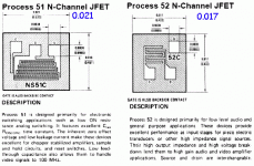
The "process" is mainly the die layout, first picture. P51 is a fairly large die with a fairly large JFET on it. P52 is a slightly smaller die with a much smaller JFET on it.
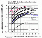
This gives a *spread* of curves, second picture. All the curves are much the same shape. Where a specific device falls left-to-right (Vgs) depends on "baking", time temp and chemistry (not precisely controlled). But the P51 curves lie 10X higher in current than the P52 curves, because P51 is a bigger device than P52.
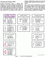
But what do you know about picking? They give you a "Proper JFET" table, third picture. JFETs can be good for 100MHz, so our <100KHz audio is Low Freq and we want Low Noise. Buying N-type Singles, we are led to P51 as one suggestion. However this is a 10mA-100mA Igss part. If we realize we may run nearer 1mA, we may look at General Purpose Amps and P52 is a suggestion.
I never found "Process" to be much help (good insight thought). There's some trends: P53 must be a teeny device which makes sense for low-low Gate leakage- indeed that is what P53's description shows and suggests. P58 is a fat beast and parts from the right end of the curve may be low-R switches (and cost more due to large 3-row die).
But we have to buy *parts*, not processes. A part is selected from a Process and the left, center, or right areas of the spread curve. Then further sorted for breakdown, leakage, or other valuable features. Then put in a Package, giving dissipation and pinout. Yes, if say 2Nxxxx is "almost right", you might look up its process and find similar parts with the difference you want. I've never done that.
The "process" is mainly the die layout, first picture. P51 is a fairly large die with a fairly large JFET on it. P52 is a slightly smaller die with a much smaller JFET on it.
This gives a *spread* of curves, second picture. All the curves are much the same shape. Where a specific device falls left-to-right (Vgs) depends on "baking", time temp and chemistry (not precisely controlled). But the P51 curves lie 10X higher in current than the P52 curves, because P51 is a bigger device than P52.
But what do you know about picking? They give you a "Proper JFET" table, third picture. JFETs can be good for 100MHz, so our <100KHz audio is Low Freq and we want Low Noise. Buying N-type Singles, we are led to P51 as one suggestion. However this is a 10mA-100mA Igss part. If we realize we may run nearer 1mA, we may look at General Purpose Amps and P52 is a suggestion.
I never found "Process" to be much help (good insight thought). There's some trends: P53 must be a teeny device which makes sense for low-low Gate leakage- indeed that is what P53's description shows and suggests. P58 is a fat beast and parts from the right end of the curve may be low-R switches (and cost more due to large 3-row die).
But we have to buy *parts*, not processes. A part is selected from a Process and the left, center, or right areas of the spread curve. Then further sorted for breakdown, leakage, or other valuable features. Then put in a Package, giving dissipation and pinout. Yes, if say 2Nxxxx is "almost right", you might look up its process and find similar parts with the difference you want. I've never done that.
Attachments
When I test a bunch of Fairchild J113s, I routinely see a 5-to-1 spread of Idss.
In current batches of that Fairchild part, I'm not seeing that. Out of couple
thousand parts, a few are maybe 14 mA, and the bulk are 19-20 mA or so, with
a few at 22 or 23. Nothing outside that, and they are not all from the same
boxes.
Maybe they learned something from Toshiba....
It takes a lot of degeneration to get them down to the 10 mA or so that the amp works with. If you don't take that approach, the Idss figures with the voltages involved will exceed dissipation limits of the parts.
Papa, you say nothing about cascodes...
[emoji6]
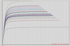
I asked myself, how many parts can I test in 10 minutes? The answer is: 31 parts. Here they are: VDS on the horizontal axis, IDS (in mA) on the vertical axis. Vgs=0 in all cases. The flat zone is the number everybody calls "Idss".In current batches of that Fairchild part, I'm not seeing that [a 5-to-1 spread in Idss]. Out of couple thousand parts, a few are maybe 14 mA, and the bulk are 19-20 mA or so, with a few at 22 or 23. Nothing outside that, and they are not all from the same boxes.
Maybe they learned something from Toshiba....
9.5mA to 24mA in a population of only 31 units. They must send ME the ones they don't send to YOU!
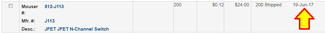
Purchased very recently, see attachment 2 (yellow)
_
Attachments
Huh. I've been latching on to NOS Siliconix J113s lately, and their IDSS is definitely on the low side, so much so that I had trouble finding lightweight enough J175s to pair with them for complements. I had to go to J176. The PN4391s I have from Fairchild are also on the hot side.
So even to use in the double differential input stages are these not good?Actually I think it is. The Idss of those parts is typically higher than you
might imagine. The J112's are typically 40-50 mA Idss and those J111's are
even higher. Same story to a lesser extent with J175's.
It takes a lot of degeneration to get them down to the 10 mA or so that the
amp works with. If you don't take that approach, the Idss figures with the
voltages involved will exceed dissipation limits of the parts. Even if they
didn't, the Drain load resistance would have to be made low to bias the
Mosfets that follow, low enough to severely impact the gain.
Either way, it's a pain in the butt. Easier to pick parts that are lower Idss
to begin with, and the K170's and J74's are still a preferred choice.
For the millionth time there is nothing wrong with Linear Systems
LSK170
LSJ74
Transistors – diyAudio Store
LSK170
LSJ74
Transistors – diyAudio Store
I'm using Fairchild_J112 + 110R source degeneration resistors, running at 5 mA per JFET, in the front end of an amplifier project. I've confirmed that this series combination results in a transconductance (gm) of 5 milliSiemens per JFET+R, both in DC testing on a curve tracer, and in AC testing with a sine wave generator and 1K load resistor on the drain.
It may be of interest that Horowitz and Hill (3rd edition, The Art of Electronics) encourage the use of the big brother device "J107" (IDSS = 100mA !) for applications in which the cost of the Interfet devices is prohibitive, but low noise is important. See p.517
It may be of interest that Horowitz and Hill (3rd edition, The Art of Electronics) encourage the use of the big brother device "J107" (IDSS = 100mA !) for applications in which the cost of the Interfet devices is prohibitive, but low noise is important. See p.517
For me the trick to getting simulations that match real devices, is to measure the real devices in the vicinity of their actual operating point in the final circuit, and extract device modeling parameters there. So for example if you're going to run your IDSS=100mA J107 at 3mA bias, extract BETA and VTO and LAMBDA from measured data that's near 3mA. Completely disregard 100mA and forget IDSS. Your circuit will never operate there.
Last edited:
In current batches of that Fairchild part, I'm not seeing that. Out of couple
thousand parts, a few are maybe 14 mA, and the bulk are 19-20 mA or so, with
a few at 22 or 23. Nothing outside that, and they are not all from the same
boxes.
Maybe they learned something from Toshiba....
Maybe they didn't. Last batch Idss about 35 mA

- Home
- Amplifiers
- Pass Labs
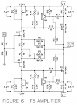
- how about using J111 J175 Jfets in F5