Let's assume that the amp, for some reason, puts out 20V DC, no speaker load attached. R3 and R4 form a path to ground with a resistance of 2.542k. The dissipated power would be P=U^2/R=0.16W. I would say that even in that worst case scenario a resistor rated about twice that power would survive pretty much indefinitely. The same math applies for R2.
Except for R32 (3W) all resistors are specified as 1/4W types. You can always go bigger.
Except for R32 (3W) all resistors are specified as 1/4W types. You can always go bigger.
just finished the amps : )
but i wonder, when i unplug the amp, music stays for another about 6-7 seconds.
as if the amp does not draw any current at all. it is totally different with my F aleph, F5 or F6 amp where music stops to play almost immediately.
how do behave your Vfet amps? Measurements seem to be ok with mine.
tnx
but i wonder, when i unplug the amp, music stays for another about 6-7 seconds.
as if the amp does not draw any current at all. it is totally different with my F aleph, F5 or F6 amp where music stops to play almost immediately.
how do behave your Vfet amps? Measurements seem to be ok with mine.
tnx
ha, i just forgot to crank the bias up  .
.
I really concentrated so much to the "before installing the Vfets" part, that i just quickly went over the last part and thought of the measuring of R32 as a kind of testing part, the value was low and i thought it was finished.
But already in bed half asleep Nelson came by and said, "you st*pid, just crank up the bias" and that was it.
Just veery cheap speakers on it but sounds fantastic!
Thanks to all, buying parts, developing the amp, make PCBs and Kits, write supernice manuals.....
. I really concentrated so much to the "before installing the Vfets" part, that i just quickly went over the last part and thought of the measuring of R32 as a kind of testing part, the value was low and i thought it was finished.
But already in bed half asleep Nelson came by and said, "you st*pid, just crank up the bias" and that was it.
Just veery cheap speakers on it but sounds fantastic!
Thanks to all, buying parts, developing the amp, make PCBs and Kits, write supernice manuals.....
third enlightment,
-cranking up bias messes your frontend offset.
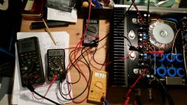
it seems that the frontend biasing is the most tolerable, and since i just got 3 multimeters, i looked up
-output offset
-vfet bias (R32 to gnd 100mV)
-frontend offset
i went back to the frontend bias and had about 1450mV to 1470mV btween T6/T7 what seemed to be ok.
everything interacts, so 4 Multimeters woudn´t be a bad idea!
, -cranking up bias messes your frontend offset.
it seems that the frontend biasing is the most tolerable, and since i just got 3 multimeters, i looked up
-output offset
-vfet bias (R32 to gnd 100mV)
-frontend offset
i went back to the frontend bias and had about 1450mV to 1470mV btween T6/T7 what seemed to be ok.
everything interacts, so 4 Multimeters woudn´t be a bad idea!
Five would be ideal actually. 2x frontend bias, 1x frontend offset, 1x bias current draw, 1x output offset. I redid the bias procedure with four DMM's once the amp settled in.
All the pots interact, but I've found that when the settings are close to ideal (frontend and output offset close to zero mV at desired bias current levels), everything tracks really well. If the bias levels differed by some amount, the interactions would be weaker it seemed. The closer both polarities came to being equally biased, the stronger the coupling of the interaction, as if the circuit snapped in somehow.
Anyway, it was really fun going back and forth between frontend and output stage, zeroing in on the desired operating point.
Attachments
...
-vfet bias (R32 to gnd 100mV)
...
I think you mean 100mV voltage drop over R32. R32 to ground should roughly be the full, unregulated supply voltage.
cablelosses?
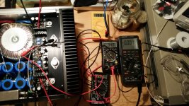
i´m still evaluating and measuring the newborn Vfet.
Today i checked the bias via the r32 to V- and it was 92mV. Measured between the testpoints on PCB.
When i go directly to the "PSU –" instead of "testpoint–" i measured 101,2mV. Thats quite a difference!
Could there be so much loss in 20cm of 1sqmm cable?
Measure the drop and see for yourself
Edit: 1sqmm would be AWG17, with about 17 Ohm per km. 17/1000*.2=3 mOhm, neglecting whatever additional resistance is added by solder joints, circuit board tracks and so on. With a DC current of 1A you should see a drop of at least U=R*I=3mV. What you're seeing is higher than that, but not unreasonable.
Edit: 1sqmm would be AWG17, with about 17 Ohm per km. 17/1000*.2=3 mOhm, neglecting whatever additional resistance is added by solder joints, circuit board tracks and so on. With a DC current of 1A you should see a drop of at least U=R*I=3mV. What you're seeing is higher than that, but not unreasonable.
Last edited:
Assembly of the Vfet amp PCB Work in progress

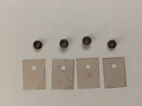
The small mosfets shown are in the TO-220FP package, so no insulator is required. You do need a bit of heatsink compound, so smear a bit on and try to achieve better coverage than in this photo. If your mosfets have an exposed metal tab then you'll need a small plastic sleeve for the holes and an insulator. These sleeves are supplied in the supplemental kit along with TO-220 mica insulators which require grease on each side.
Jim,
Toshiba's 2SK2013/2SJ313 are becoming very rare and quite expensive, therefore I plan to use Fairchild's FQP3N30/FQP3P20 MOSFETs, however these transistors have the "exposed metal tab" that you mentioned. In such cases you suggested the use of a "small plastic sleeve for the holes", that should have been included on the supplemental kit. Well, I searched for these sleeves on the kit's BOM, but could find no allusion to them!
Could you please give me a reference for those sleeves?
Odd. My kit had them, though I did not need them because I used the Toshibas.
Attachments
Oh I see!
They are part of heatsink mounting kit (4880MG-ND - vendor part number).
I don't have the supplemental kit, when I bought my VFET kit they were sold out, thus I'm gathering all the needed parts.
Could you help me with the dimensions of the nylon spacers used in the brackets holes for the VFETs?
Apparently, the VFET kit (mine was from the last batch and will take a couple of months to be delivered) includes only 8 units, so I have to track 8 more units.
Thanks henryve.
Last edited:
- Home
- Amplifiers
- Pass Labs
- Sony vFET Illustrated build guide