Hello 2 picoDumbs. Have you already assembled your circuit? On turn on, the upper depletion type FET may appear as a low-Ohm power resistor until it biases properly.
Hi Antoinel, just thinking about this a little more, both devices have zero temperature coefficient, so they bias up virtually instantly. At least that has been my experience with the Lateral mosfets. The United Carbide device also has zero temperature coefficient at the currents we are interested in (say 1A to 2A) so both devices should bias at same rate ie virtually instantly.
I probably won't get this built for quite some time to test it out, but I think it's not going to be a significant problem.
Thank you 2 picoDumbs.
Experimenting with DEF
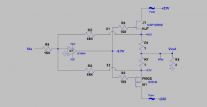
I assembled a DEF power amp per the attached schematic. I will post its pics.
1. I used DEF as a power booster for the OpAmp [LF356N] which is connected as a phase inverter.
2. Each FET idles at ~0.2A
3. The joint Vgs at idle equals [-3.7V]
4. The voltage gain of the resultant amp is ~2
5. The fuses [~0.6 A each] on the +/-23V power rail are made with small light bulbs [4 per fuse]; for a visual status at idle and during music play.
6. The power rails to the OpAmp were limited to +/-12V. This is a precaution preventing the Vgs of SJDP120R085 from exceeding its +/-15V max rating.
Here is the method I used to power it on/off.
1. Turn power on to the OpAmp.
2. Note the joint Vgs =-11.6 V.
3. Turn power on to DEF stage. Its joint Vgs stabilizes at -3.7 V.
4. No pops, or thumps were heard by a 4 Ohm loudspeaker load.
5. For turn off, follow the sequence of points 3, 2, and 1. No pops were heard.
Music sounded great and detailed. Amp was very quiet at idle. No hiss or buzz from the tweeter, and woofer respectively. I limited its voltage output across the loudspeaker during music peaks to 10 Vp-p; so as not to clip the output stage of the OpAmp.
Attachments
Very nice Antoinel
If you match the R085 and the 9240 is the need for the 1 ohm resistor eliminated?
Best
Thanks flocchini. Unfortunately, I do not have a high power Pass +/- 23 V power supply, and adequate heatsinking for my and your suggested experiments.
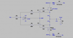
A schematic of a DEF power amp is attached. It shows that it does not use source degeneration resistors:
1. The gates of the FETs are tied together with a Vgs at ~ -3.65 V
2. The sources of the FETS are tied together, and are at 0 Vdc during idle.
3 The steady state drain current of each FET is ~0.45 A. It is sensed as a voltage drop across a 0.5 Ohm resistors which is connected to the drain of each FET.
4. The steady state dual drain voltage Vds = +/-9.5 V. I initially started at a Vds of +/-5 Vdc, and slowly increased it [with variac] while I paid attention to the light intensity of the light fuses which was close to full brightness.
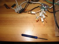
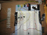
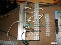
One picture shows the OpAmp circuit. A second picture shows the DEF power output stage on heat sink. The lower FET is IRF9140 MOSFET. A third picture shows the lit light fuses, and the 0.5 Ohm sense resistors to their left.
The amp sounds great at low level music play. No hiss or hum emanated from the loudspeaker.
I will continue to increase +/- Vds carefully. I expect the source currents [0.45A] to eventually plateau with increasing Vds; because both FETs are voltage variable current sources [pentode-like electrical characteristics].
1. The gates of the FETs are tied together with a Vgs at ~ -3.65 V
2. The sources of the FETS are tied together, and are at 0 Vdc during idle.
3 The steady state drain current of each FET is ~0.45 A. It is sensed as a voltage drop across a 0.5 Ohm resistors which is connected to the drain of each FET.
4. The steady state dual drain voltage Vds = +/-9.5 V. I initially started at a Vds of +/-5 Vdc, and slowly increased it [with variac] while I paid attention to the light intensity of the light fuses which was close to full brightness.
One picture shows the OpAmp circuit. A second picture shows the DEF power output stage on heat sink. The lower FET is IRF9140 MOSFET. A third picture shows the lit light fuses, and the 0.5 Ohm sense resistors to their left.
The amp sounds great at low level music play. No hiss or hum emanated from the loudspeaker.
I will continue to increase +/- Vds carefully. I expect the source currents [0.45A] to eventually plateau with increasing Vds; because both FETs are voltage variable current sources [pentode-like electrical characteristics].
Attachments
Hi, I would like to know if you evaluate the output stage in mono?
It seems to me that stereo could be distracting.
Also, since the goal is to determine the sonic impact of the transistors, i suppose there is no feedback applied to the output stage, but can local feedback be applied to the VAS used to drive the output transistor?
In his burning amp presentation, Mr Pass mention that he has setup specifically designed to allow him to listen to output stages. But does not provide much details.
I would imagine the XP30 is part of the set up:
http://www.diyaudio.com/forums/pass-labs/191392-pass-labs-new-product.html#post2616425
Cheers,
Dennis
http://www.diyaudio.com/forums/pass-labs/191392-pass-labs-new-product.html#post2616425
Cheers,
Dennis
Hi, I would like to know if you evaluate the output stage in mono?
It seems to me that stereo could be distracting.
Also, since the goal is to determine the sonic impact of the transistors, i suppose there is no feedback applied to the output stage, but can local feedback be applied to the VAS used to drive the output transistor?
In his burning amp presentation, Mr Pass mention that he has setup specifically designed to allow him to listen to output stages. But does not provide much details.
Hello BaffleChallenged. The power amps described in my posts above defined the valuable joint Vgs = -3.6Vdc which gave equal drain current in each FET at equal drain-source voltage for each FET. This resulted in the joint sources of the FETs to sit at a voltage ~0 Vdc for direct coupling to a loudspeaker.
In an ongoing experiment, the joint Vgs of the FET will be biased via an independent circuit at -3.6 Vdc. The music signal will be capacitor coupled and merged with this bias at the joint gates of the FETs. This DEF power booster will stand alone in the resultant power amp as intended; so as to listen to it without overall negative feedback.
DEF with 2sk82
Here is a model with 2sk82 and a p channel part from the spice library. We reach 0 V offset when they both idle at around 912mA.
Included is the spice model i used for 2sk82
and a picture of the FFT graph for 7 Watts into 4 Ohms.
Let me think how you evaluate its performance.

[/ATTACH][/ATTACH]
Here is a model with 2sk82 and a p channel part from the spice library. We reach 0 V offset when they both idle at around 912mA.
Included is the spice model i used for 2sk82
and a picture of the FFT graph for 7 Watts into 4 Ohms.
Let me think how you evaluate its performance.
[/ATTACH][/ATTACH]
Attachments
Last edited:
Here is a model with 2sk82 and a p channel part from the spice library. We reach 0 V offset when they both idle at around 912mA.
Included is the spice model i used for 2sk82
and a picture of the FFT graph for 7 Watts into 4 Ohms.
Let me think how you evaluate its performance.
View attachment 589103
[/ATTACH][/ATTACH]
Hello jostwid. Interesting DEF whereby a SIT [triode-like] and a MOSFET [pentode-like] cooperate to make a power booster. Is a Vgs= -7V for the indicated MOSFET high?
Hello Antoinel
Happy new year!
You are right. After a look at the datasheet it is obvious that -7V for this particular Mosfet would mean its sure death. It is a small power device. But it works nicely in Spice....
I also tried other Mosfets like IRFP9240. We reach 0 V offset when both devices idle at 1.93 A. This would work but dissipation is unnecessarily high and for sure the upper limit for the 2sk82 (23 x 1.93 = 44 W)
Hello Antoinel
Happy new year!
You are right. After a look at the datasheet it is obvious that -7V for this particular Mosfet would mean its sure death. It is a small power device. But it works nicely in Spice....
I also tried other Mosfets like IRFP9240. We reach 0 V offset when both devices idle at 1.93 A. This would work but dissipation is unnecessarily high and for sure the upper limit for the 2sk82 (23 x 1.93 = 44 W)
Hello jostwid. Thank you for your well wishes. Happy 2017 to you, and to our diyaudio colleagues. In an earlier post, diyer wrenchone noted that United Silicon Carbide has depletion N-FETs [like UJN1205K] which has similar characteristics to SemiSouth's SJDP120R085. I pay attention to the parameter Vgs threshold which for R085 is about -5Vdc, and for UJN1205K is -6Vdc. The lower power UJN1208K has a Vgsth =-7 Vdc, which may possibly be paired with 2SJ28 P-SIT like you were simulating with 2SK82. Furthermore, in the BAF 2016 presentation part 2 by Mr. Pass, he mentionned IXYS regarding DEF. IXYS has depletion N-Mosfets which have Vgs threshold ~-4Vdc.
IXYS depletion mode like: http://ixapps.ixys.com/DataSheet/DS99192B(IXTH-T20N50D).pdf
or the monster: http://ixapps.ixys.com/DataSheet/IXFN50N120SK.pdf
Sent from my iPhone using Tapatalk
or the monster: http://ixapps.ixys.com/DataSheet/IXFN50N120SK.pdf
Sent from my iPhone using Tapatalk
Experimenting with DEF
N.B. The above statement in my previous post will not make a DEF; because it suggests using two depletion devices. My apology for this mistake as it is out of place.
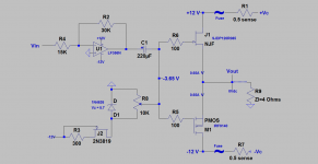
The attached schematic is the status of a DEF amp which does not use overall loop feedback:
1. The generator of negative bias to the DEF joint gates is shown at the bottom left of the view. A JFET [2N3819] constant current source drives a 5.7v Zener. The Zener voltage is trimmed with a 10K pot so as to give the exact value of -3.65 V found earlier. This value was stable throughout the experiment.
2. The music preamp is an OpAmp inverter of gain = 2. It can be anything else. Its output is capacitor coupled to the joint gates of DEF. Best to use the recommendation of Mr. Cordell [BAF 2016 presentation] for this capacitor.
Here is turn the sequence:
1. Turn on the +/-12V low power supply to the OpAmp and bias generator.
2. Turn on the high power variable power supply to DEF. Start at +/- 5 Vdc as a precaution.
3. A load to DEF is not needed during this adjustment. The output offest was ~40 mV.
4. Increased +/- Vdc to DEF slowly [with variac] to +/-12 V to get a 0.65 A drain current in each FET.
5. The output offset hovered at a stable ~5 mV.
6. The drain currents in DEF drifted up a bit as the heat sink warmed up. An increase of Id ~20 mA was noted.
This amp sounded great in a 4 Ohm shelf loudspeaker. Highly detailed without hiss or hum. I kept the music peaks within 6 Vp-p. No pops in the loudspeaker when the high power supply was turned off.
I will correlate +/- Id with +/-Vds and report.
The lower power UJN1208K has a Vgsth =-7 Vdc, which may possibly be paired with 2SJ28 P-SIT like you were simulating with 2SK82. .
N.B. The above statement in my previous post will not make a DEF; because it suggests using two depletion devices. My apology for this mistake as it is out of place.
The attached schematic is the status of a DEF amp which does not use overall loop feedback:
1. The generator of negative bias to the DEF joint gates is shown at the bottom left of the view. A JFET [2N3819] constant current source drives a 5.7v Zener. The Zener voltage is trimmed with a 10K pot so as to give the exact value of -3.65 V found earlier. This value was stable throughout the experiment.
2. The music preamp is an OpAmp inverter of gain = 2. It can be anything else. Its output is capacitor coupled to the joint gates of DEF. Best to use the recommendation of Mr. Cordell [BAF 2016 presentation] for this capacitor.
Here is turn the sequence:
1. Turn on the +/-12V low power supply to the OpAmp and bias generator.
2. Turn on the high power variable power supply to DEF. Start at +/- 5 Vdc as a precaution.
3. A load to DEF is not needed during this adjustment. The output offest was ~40 mV.
4. Increased +/- Vdc to DEF slowly [with variac] to +/-12 V to get a 0.65 A drain current in each FET.
5. The output offset hovered at a stable ~5 mV.
6. The drain currents in DEF drifted up a bit as the heat sink warmed up. An increase of Id ~20 mA was noted.
This amp sounded great in a 4 Ohm shelf loudspeaker. Highly detailed without hiss or hum. I kept the music peaks within 6 Vp-p. No pops in the loudspeaker when the high power supply was turned off.
I will correlate +/- Id with +/-Vds and report.
Attachments
IXYS depletion mode like: http://ixapps.ixys.com/DataSheet/DS99192B(IXTH-T20N50D).pdf
or the monster: http://ixapps.ixys.com/DataSheet/IXFN50N120SK.pdf
Sent from my iPhone using Tapatalk
Thank you for this info.
After the VFETs have been put to bed, I think I will do something like that.
")
Experimenting with DEF
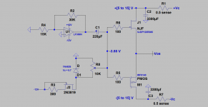
The DEF amp which ascribes to the attached schematic was used to correlate s+/-Id with +/-Vds of its power output FETs. Please note the minor changes in it.
1. Vin port to the OpAmp was grounded.
2. The light fuses were removed.
3. Added 3,300uF filter capacitors at the drain ports of the FETs.
4. The power output of the amp was not loaded.
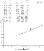
Power on to the amp was described in the previous post. The drain voltages were started at+/-5V. The amp was allowed to stabilize for 2 minutes. The voltage across the sense resistors multiplied by two gave +/-Id. Vos and its polarity were noted. This sequence of steps was repeated by increasing +/-5V by 1V increments till +/-15 V. The resultant data are shown in the attachment:
1. The individual +/- Vd were identical in value.
2. The individual resultant +/-Id were identical in value.
3. The offset voltage at the power output [Vos] was <50 mV. It changed polarity from minus to plus with increasing +/-Vd.
The graph of Id [in Amps] versus Vd = Vds [Volts] is a straight line. In a past post, I had hoped or expected that drain current will eventually plateau or become ~parallel to the x axis with increasing +/-Vd. I am not sure now if Id will plateau at higher values or continue its straight line ascent. A straight line from +/-5 V to the +/23 V operational value is relevant.
The heat sink became lukewarm during the progression of Vd from +/-5 V to +/-15 V. After noting the data for Vd = +/-15 V, it was lowered to +/-10 V and the resultant data quickly noted. It is the [*] data point on the graph which reflects a +/-30 mA drift; most probably due to the higher temperature of the heat sink [or devices] than firstly measured at +/-10 Vd.
The DEF amp which ascribes to the attached schematic was used to correlate s+/-Id with +/-Vds of its power output FETs. Please note the minor changes in it.
1. Vin port to the OpAmp was grounded.
2. The light fuses were removed.
3. Added 3,300uF filter capacitors at the drain ports of the FETs.
4. The power output of the amp was not loaded.
Power on to the amp was described in the previous post. The drain voltages were started at+/-5V. The amp was allowed to stabilize for 2 minutes. The voltage across the sense resistors multiplied by two gave +/-Id. Vos and its polarity were noted. This sequence of steps was repeated by increasing +/-5V by 1V increments till +/-15 V. The resultant data are shown in the attachment:
1. The individual +/- Vd were identical in value.
2. The individual resultant +/-Id were identical in value.
3. The offset voltage at the power output [Vos] was <50 mV. It changed polarity from minus to plus with increasing +/-Vd.
The graph of Id [in Amps] versus Vd = Vds [Volts] is a straight line. In a past post, I had hoped or expected that drain current will eventually plateau or become ~parallel to the x axis with increasing +/-Vd. I am not sure now if Id will plateau at higher values or continue its straight line ascent. A straight line from +/-5 V to the +/23 V operational value is relevant.
The heat sink became lukewarm during the progression of Vd from +/-5 V to +/-15 V. After noting the data for Vd = +/-15 V, it was lowered to +/-10 V and the resultant data quickly noted. It is the [*] data point on the graph which reflects a +/-30 mA drift; most probably due to the higher temperature of the heat sink [or devices] than firstly measured at +/-10 Vd.
Attachments
- Home
- Amplifiers
- Pass Labs
- DEF Amp