OK, I updated the schematics with the transistors.
Still need to remove R21 and R22 since the manual states that there is no degeneration in any stage.
Unfortunately 2SC4793 and 2SA1837are no longer available.
Luckily, I bought a few hundred of each.

But, we could use anything (e.g. BC550/560) for cascodes in this case since dissipation won't be a problem with the fairly low (<30V) rails we expect to use.
Last edited:
Still need to remove R21 and R22 since the manual states that there is no degeneration in any stage.
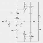
Hold on to your hat... I think the circuit configuration is different than what we previously thought....
As you just said, there are no de-generative feedback resistors.
With this information at hand, I think the circuit is something like this:

Last edited:
Devices in pic #237 probably are bridge rectifiers and not MosFets.
It looks as if PL now uses a supply with CRC-smoothing.
Interesting, but if they are rectifiers, where are the gain devices then? and why would the rectifiers need such a huge heat sink?
...I am not sure.... I think these might be the output Push/Pull Q's..
Hold on to your hat... I think the circuit configuration is different than what we previously thought....
As you just said, there are no de-generative feedback.
With this information at hand, I think the circuit is something like this:
The manual states that the amp is three stages, and the circuit you've just shown is only two. At least using the Pass Labs forum method of counting, where we don't count cascodes as a separate stage.
The manual states that the amp is three stages, and the circuit you've just shown is only two. At least using the Pass Labs forum method of counting, where we don't count cascodes as a separate stage.
-----------------------------
Yes, my sentiments exactly...
Please look at post #245 above...

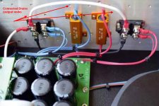
Check the orientation again - those are sources connected together.
Please explain... I am not sure I follow...
Attachments
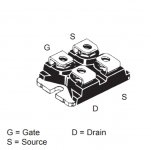
The mounting holes on the MOSFETs have one round hole in a solid metal side and one routed hole through the metal. You can see the right-hand MOSFET has the routed hole on the right side. The gate and drain connections are on the same side as the routed hole, while the source connections are on the solid side with the round hole.
The mounting holes on the MOSFETs have one round hole in a solid metal side and one routed hole through the metal. You can see the right-hand MOSFET has the routed hole on the right side. The gate and drain connections are on the same side as the routed hole, while the source connections are on the solid side with the round hole.
------------------------------------------
My apologies, but your explanation does not make things any more clear.
Could you please use the picture above?
What do you mean "the round hole in a solid metal side" as opposed to "one routed hole through the metal"?
Last edited:
Dear Alexiss:
One hole is actually a slit, and the other is a hole. The gate and drain are on the side of the slit, and the sources are on the side of the hole.
So the sources (left side of MOSFETs in the picture of the XA25) are connected together, and on the right sides of the MOSFETs are drain and gate.
The thing that is fooling us here is that both wires on the right side are red (respective blue), but you can see that one wire is thicker than the other - the thicker one is the drain, the thinner one the gate.
Unfortunately, I can't quite read the print on the PCB where Drain an Gate go to ...
Best regards,
Claas
P.S.: Seems like we crossposted a bit also
Last edited:
The red leads and blue leads are actually separate the sources are indeed the outputs. I had to check production the picture is confusing.
Dear wayne:
Are the other terminals of the sources (the black wire) connected together also ?
Regards,
Claas


The red leads and blue leads are actually separate the sources are indeed the outputs. I had to check production the picture is confusing.
----------------------------
OK, now I got the confirmation that I needed. Thanx Mr Wayne.
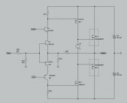
Then the possible solution once again becomes:
As can be seen, the input resistors are given values, and the degenerative local feedback resistors are gone every where.
It would be interesting to see if this is correct or not..
Attachments
- Home
- Amplifiers
- Pass Labs
- Pass XA25?