I don't need a big amp like this but liked the looks of that current source. I wish someone would make a small circuit board for that current source.
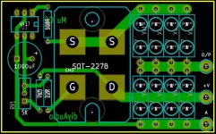
I have made a PCB for the CCS.
Regards,
Dan
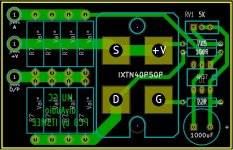
Something like this? I need to check it over with fresh eyes tomorrow, when it's ok I'll post the gerbers.
I like the flexibility of your design.
Regards,
Dan
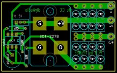
With fresh eyes, I added the missing track, then noticed that the SOT-227B datasheet I was using had the gate and drain reversed 
New layout, Iv'e checked it over a number of times, looks ok... I zipped up the gerbers then uploaded to JLC PCB, now waiting for delivery
New layout, Iv'e checked it over a number of times, looks ok... I zipped up the gerbers then uploaded to JLC PCB, now waiting for delivery
Attachments
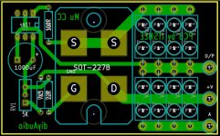
Itsmee,
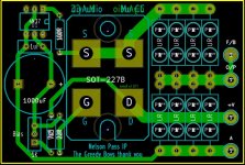
I'm resting after a great day at BAF and I've been staring at your pcb design for a long time, checking the amplifier schematic and the IXFN data sheet, and it looks to me that you have the source and drain connections reversed. As far as I can tell, you are sending 60V to the Source and then outputting out of the Drain. But it should be the other way around. The 60V goes to the Drain and outputs out of the Source.
As I said, I have been looking at it for a while so I don't believe that I am wrong. I mean, I am questioning myself over this but in the end it looks backwards to me.
I apologize if I'm completely out to lunch.
Ben
...it looks to me that you have the source and drain connections reversed...
Doh! Good catch, thank you. Hopefully third time lucky.
Last edited:
Here's my final version of the CCS. I modified it so I could use the following for R4 and R5.
TWW10JR20E Ohmite | Mouser Canada
Regards,
Dan
TWW10JR20E Ohmite | Mouser Canada
Regards,
Dan
Attachments
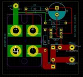
Hopefully it's right this time.
Bad news!
Something that I didn't catch last time - pin 5, not pin 6, of the 4N35 connects to the 1000uF cap positive terminal.
In your switch-around of Drain and Source, some of the connections were messed up. Your 4N35 pins 2 and 4 and 1000uF cap negative is now connected to the speaker out (O/P). It should be connected to "A" on your board.
Maybe fourth time lucky.
I owe Ben a cold beverage. He caught a flaw on my schematic!
BAF 2020? I've been hanging out with your fellow Torontonian Dennis Hui here in SF.
Simple circuit, can't believe I keep cocking it up!
Being a bit stupid i always follow the workflow: schematic > netlist > pcb. Even for something simple. In the long run it is better for documentation and maintenance. It also excludes any possibility for the pcb not to match the schematic.
...i always follow the workflow: schematic > netlist > pcb...
That's the correct way; working free hand isn't usually a problem as I would normally print the schematic and component pin-outs as I layout; then check off the circuit layout against the schematic using highlight pen as I go.
At the moment, I don't have a working printer
I should buy one, better still, learn to do it properly

- Home
- Amplifiers
- Pass Labs
- 50w Single-Ended BAF2015 Schade Enabled