Pass DIY Addict
Joined 2000
Paid Member
Hi Graeme, Thanks for the link. I remember reading through that before - perhaps it makes a little more sense to me after letting some time go by... I have 3 amps that I want to convert to JFET inputs and I have three matched quads of 2SK170's from Spencer.
So now I have a bunch of detail oriented questions:
1) You used four 2SJ109's in conjunction with four ZTX550's. This is a little confusing to me, since it looks like others have just used four matched 2SK170's (directly replacing the 109's in your diagram). Are the 550's necessary if I'm using the 170's?
2) I can't seem to find a definitive diagram for N-channel JFETs. In the schematic that you linked, is it the Source or the Drain that is opposite of the Gate? Some sources I've found indicates that at low signal levels, the Source and Drain are interchangeable... I guess more directly, is it the Drain or the Source of the 109's that is connected to the Drain of the 9610 above?
3) You seem to have made a number of other changes such as the input network as well as various resistor values (R16, R46), R22 was omitted, and you've added a diode to ground at the 550's. I don't understand the significant and purpose of these changes. Are they necessary if I use 170's?
4) I presume the 109's on the "left" side of the diagram need to be thermally coupled with one another, as do the pair on the "right" side of the circuit. Is this correct? Is the same true for the 550's on each side? I have some of the dual JFET heat sinks that were sold here at DIYAudio some time ago...
I'm sure I'll have other questions shortly.
Thanks,
Eric
Last edited:
Hi Graeme, Thanks for the link. I remember reading through that before - perhaps it makes a little more sense to me after letting some time go by... I have 3 amps that I want to convert to JFET inputs and I have three matched quads of 2SK170's from Spencer.
So now I have a bunch of detail oriented questions:
1) You used four 2SJ109's in conjunction with four ZTX550's. This is a little confusing to me, since it looks like others have just used four matched 2SK170's (directly replacing the 109's in your diagram). Are the 550's necessary if I'm using the 170's?
2) I can't seem to find a definitive diagram for N-channel JFETs. In the schematic that you linked, is it the Source or the Drain that is opposite of the Gate? Some sources I've found indicates that at low signal levels, the Source and Drain are interchangeable... I guess more directly, is it the Drain or the Source of the 109's that is connected to the Drain of the 9610 above?
3) You seem to have made a number of other changes such as the input network as well as various resistor values (R16, R46), R22 was omitted, and you've added a diode to ground at the 550's. I don't understand the significant and purpose of these changes. Are they necessary if I use 170's?
4) I presume the 109's on the "left" side of the diagram need to be thermally coupled with one another, as do the pair on the "right" side of the circuit. Is this correct? Is the same true for the 550's on each side? I have some of the dual JFET heat sinks that were sold here at DIYAudio some time ago...
I'm sure I'll have other questions shortly.
Thanks,
Eric
OK, I'll do my best and answer your questions in order. I will be talking about one channel here when I make circuit references.
1) The 2SJ109BL is dual transistor part. It's the equivalent of two 2SJ74BL's. I created the diff pair (I'm talking one channel) by putting one transistor from each 2SJ109 on each side of the diff pair. I hope that makes it clear. Please note that I didn't match the two 2SJ109BL's (4 transistors) to each other. I just took the next 2SJ109BL from the bag as I was assembling the PCB's.
Please note here too that the 2SJ109 and 2SJ74 are P channel parts, just as the 9610 is a P channel MOSFET. That is what you must use. The 2SK170 is an N channel part and won't work here.
The cascode transistors aren't absolutely necessary. I used them for several reasons: 1) I believe that 8V-10V is a sweet spot for the J74/K170 parts, 2) thermal dissipation on the JFET's is kept down to almost nothing so possible drift is reduced/eliminated and thermal coupling is not necessary, 3) I wanted to avoid JFET source degeneration resistors in order to keep the gain up but I needed a way to avoid current hogging, and 4) the maximum Vds for the 2SJ74 is 25V on the data sheet and the AX100J uses 27V rails. I have since found out from NP that these parts are actually OK to higher voltages. But I didn't know that at the time. And even then these were rare and valuable parts.
2) The P channel JFET symbol I used shows the gate close to the source. The sources of the JFET's are connected to the drain of the 9610. The source and drain of the 2SJ109/2SJ74 can be interchanged but I always connect them as shown on the data sheet.
3) I will need to get back to you about the specific resistor designators you reference. I need to check a couple of things on that. The resistor and zener that are connected to the ZTX550's form the voltage reference for these cascode transistors.
4) I didn't thermally couple anything. The cascodes keep the dissipation of each JFET down to 40 milliwatts (P = 8V * 5ma), so IMO all the JFET's are staying at room temp. So no need to thermally couple. I am seeing no drift so I think I'm good. A lot of people here are big believers in thermal coupling. If you want to do it then go ahead. Bottom line it won't hurt and it may help. If it does improve things then definitely let me know.
If I've been unclear let me know.
Graeme
Last edited:
Pass DIY Addict
Joined 2000
Paid Member
Another question: if I use a quad of sk170's to replace the 9610 differential, what Ids should I aim for with matching? Does this matter, given that I can adjust the bias with R23/R25?
The matched sets that I have are matched at about 8.5mA. Will these work, or should I get matches as a different Ids?
The matched sets that I have are matched at about 8.5mA. Will these work, or should I get matches as a different Ids?
Hi Eric,
You can't use 2SK170's. They are N channel parts and are the wrong polarity. You must use P channel parts. That means 2SJ74BL's or 2SJ109BL's.
I substituted two 2SJ74BL parts (2SJ109BL - same specs) for each 9610. So if the 9610 is running 10ma of bias then each JFET will have 5ma of bias. So you need to pick JFET with an Idss higher than that. I'd pick an Idss of 7ma or more. Almost any BL part would work here. The Idss match should be within 10%.
I did what I did to avoid having to change the bias in the diff pair.
Graeme
Pass DIY Addict
Joined 2000
Paid Member
Hi Eric,
OK I've reviewed the schematics. So here are some comments about those resistor value changes.
R22 is easy. JFET's don't need the 220 ohm gate stopper resistors - at least not when there's just one (or a couple in parallel). Note too that the input protection diodes were deleted as well - not needed with JFET's.
R16 and R46 (and a few others in the AX100J) are values that came from schematics of the pass Labs X5 and X2 circuits that NP posted briefly here 'once-upon-a-time'. These are/were JFET input supersymmetric circuits. Some of the other value changes were calculated by me as a result of updating R16 and R46 etc.
Graeme
Pass DIY Addict
Joined 2000
Paid Member
Thank you for the continuing details, Graeme! This is very helpful! I'm sure I'll have more questions as I think about this more carefully. Time to start drawing things out to see how best to implement these changes. My first thought is to add a small secondary perf-board to hold the new transistors...
Hi Eric,
you could also have a look here:
http://www.diyaudio.com/forums/pass-labs/98763-alephj-x.html
Depending on the amount of input fets (2 or 4) you will need to change the drain resistors from 392R to something like 910R to account for the reduced bias.
You will also need to change the current source resistors to be able to set a lower bias if you go from 20mA to 10mA
And last but not least you need to change the McMillan resistors (start with the double value you have now)
I don't think I changed anything else. Coupled the input JFets to each other and used a 10R pot as a replacement for source resistors and to set the relative dc offset.
William
Pass DIY Addict
Joined 2000
Paid Member
Temperature compensation
Hi,
today I tried to put some PTC's in the current source for the input diff pair.
I've used KTY81-110 as suggested by Salomon (thanks again!).
Until now the current source was build around Q6a (IRF9610) with 3x2.9V zeners and the following values for the resistors:
R24 2k7
R26 680R
VR2 200R
I've replaced R24 with a KTY81 and a 1k5 or 1k2 resistor, the rest remained unchanged.
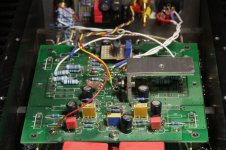
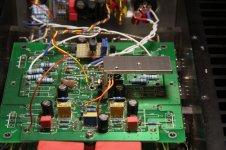
The PTC is coupled to the IRF9610 which is coupled to the top of the case.(see pics)
Well, it seems to work fine. The calculated 1k5 seems a bit high (the absolute DC get's more negative during warmup) so I've put 1k2 in the other channel which is better. I'll watch some real cold starts and do some long runs to decide which one is better or if I have to go even lower.
This setup will probably only work for my amp but with a different combination of resistors it should also be possible to make it work for IRF9610 or quod JFet inputs.
William
Hi,
today I tried to put some PTC's in the current source for the input diff pair.
I've used KTY81-110 as suggested by Salomon (thanks again!).
Until now the current source was build around Q6a (IRF9610) with 3x2.9V zeners and the following values for the resistors:
R24 2k7
R26 680R
VR2 200R
I've replaced R24 with a KTY81 and a 1k5 or 1k2 resistor, the rest remained unchanged.
The PTC is coupled to the IRF9610 which is coupled to the top of the case.(see pics)
Well, it seems to work fine. The calculated 1k5 seems a bit high (the absolute DC get's more negative during warmup) so I've put 1k2 in the other channel which is better. I'll watch some real cold starts and do some long runs to decide which one is better or if I have to go even lower.
This setup will probably only work for my amp but with a different combination of resistors it should also be possible to make it work for IRF9610 or quod JFet inputs.
William
Attachments
Pass DIY Addict
Joined 2000
Paid Member
Thanks for sharing your results, William.
I am curious to hear how offset tracks with temperature now... I am planning to attach the KTY81's directly to my main heat sink right between two of the output mosfets - though I haven't worked out the mechanics just yet.
By the way: what caps are you using for your input? Currently, I'm using cheap Dayton caps from PartsExpress.com, but was looking to replace them with Intertechnik audyn true copper cap. I keep putting it off due to their cost...
Last edited:
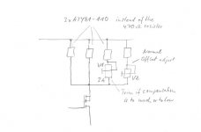
Fixing all Aleph-X Offsets
I am sure with with the right combination of PTC it is possible to completely compensate the temperature drift.
It is my opinion the type of zener diodes does not make such a big difference.
I only can speak for the normal version of the Aleph-X circuit with IRF9610.
For all who use a Aleph-X with JFETs I am sure William will find a good part combination.
I use 2 pieces of the KTY81 PTC. I chose this device because it has a very linear characteristic.
With three pieces and a trimmer in series of the third part it is possible to compensate for the temperature drift completely.
Please see my attachement
The new trimmer is for right adjusting between over compensation and under compensation.
Try a 2K trimmer and begin the adjustment with adjusting the biggest value.
First you have to adjust he normal offset trimmer and to judge the remaining offset drift from cold to warm.
If the PTCs don`t compensate completely the temperature drift, you have to decrease the adjustment of the additional 2k trimmer to a smaller value.
The right adjustment is a combination of the adjustment of both trimmers.
If changing the adjustment of the 2K trimmer it is important immediately to re-adjust the normal offset trimmer to zero offset.
A good thermal coupling of the PTCs to the temperature of the output FETs (heat sink) is very important !
*
We are speaking here about the offset that we measure from each output pin to ground. This one you can compensate with the PTCs.
The offset measured between both output pins is depending of the matching of the IRF9610, its Drain Resistors and the matching of the parts of the output stages.
If you want to easy get a little remaining offset to zero it is possible to solder a resistor over the Drain resistor (390R) who you can measure the bigger voltage of both IRF9610.
Try to determine the right value with first solder a 10K trimmer over the Drain resistor.
Begin to trim from highest value (10K or more) to a lower value.
If you measure 0mV over both output pins you have found the right value. Solder out the trimmer and measure the value. Now you can change it against a normal resistor and solder it over the normal Drain resistor. This choice is better for long time offset stability.
Now the offset between the output pins allways will be stable at 0mV or less than 10mV . Cold or warm amp will not make any difference.
*
Sorry for my bad English, but it is important for me to make this information accessible to all persons in the world who love the Aleph-X like I love it.
*
Here you find some pictures of my Alep-X amp.
Class A monster: Aleph-X by Horst Wolf Audio Tweak
Attachments
Hi,
had the amps on quite long last night and measured around -2V of offset. Measured again this morning (cold) and had around 3V in the left channel and 1.5V on the right channel. So the voltage swing is around 5V left and 3,5V right (remember there are different R24 in both amps)
This means, that I have to raise the influence of the PTC a bit more, lower
R24 and raise R26.
Before the swing was around 8V (R46/47 being 22k). Changing R46/47 to 27k would have changed this to around 10V.
@Eric: I coupled the KTY to the current source fet as I found out this had by far the biggest influence on absolute DC Offset. Cooling and heating the outputs, diff pair and some more had almost no influence.
On the input are a pair of black gate F? (the red ones, bipolar)
@Graeme: Yes I would because it means you can raise the value of McMillan resistors which (I think) has a positive influence on sound quality.
I did install the 3 zeners but somehow that didn´t work as it should have (giving a negative tempco)
William
Hi Horst,
we somehow posted at the same time")
Out of the results of the two amps I can calculate a third setting to get the drift to (almost zero). Will be something like R24=680R plus KTY and R24 = 820R. Will try this evening.
In my amp the temperature influence of the output fets is almost zero. I've put one side of the amp (current source and output) on one heatsink and the other side on the other heatsink. This way Vgs changes over temp will compensate each other.
William
we somehow posted at the same time
Out of the results of the two amps I can calculate a third setting to get the drift to (almost zero). Will be something like R24=680R plus KTY and R24 = 820R. Will try this evening.
In my amp the temperature influence of the output fets is almost zero. I've put one side of the amp (current source and output) on one heatsink and the other side on the other heatsink. This way Vgs changes over temp will compensate each other.
William
Hi William,
i am sure both stages have a temp offset drift
It is clear that the drift of the input current source who changes the Drain voltage of the IRF9610 has more effect because this changing of the drain voltage will be multiplied by the gain of the output stage.
It may be a good idea to be heated driver or heated input current source stage taking as reference temperature for the PTC
For me it was mechanically easier to take the temperature output stage as the reference.
I think with both variants you get a good offset compensation.
Hi,
tried another combination yesterday. R24 750R, R26 820R. Voltage swing is under 1 Volt now but..........
As I discovered a few years ago (and forgot in the meantime) the absolute DC Offset depends on the mains voltage (at least in my amps). If the voltage goes up, the absolute offset goes negative and vv. This also explains the little jumps (0,5-1V) I see when observing the abs.dc offset.
This means more negative late at night and more positive early at night. I will see if I can measure it with a variac from 220-240V.
I will also try to up the McMillans from 27k to 33k.
William
Hi William,
very interesting!
I am sure you will find the best values for a perfect compensation.
Maybe its better to use only one of piece of the PTCs because you a using a JFET stage if you get over compensation.
Using the normal IRF9610 circuit it is not possible to get over compensation.
If users with IRF9610 want to make a full compensation, the have to take three pieces of the PTCs and solder the second in series with a trimmer. See my other post.
I am also interrested how it sounds with the bigger values of the McMillans.
Thank you for all and good luck.
Horst
Hi,
just found something I wrote in 2006.........
QUOTE=wuffwaff;867384]Hi,
it does contribute since abs. dc offset is set with the neg. rail as a reference. When this changes, abs. dc changes.
In my amp ca. 3V of mains (232-229) change, changes offset by 1.5V
William[/QUOTE]
Will still try if this is also true for the Jfet input with larger drain resistors.
@Horst, the bigger McMillans do sound better.
William
Hi,
just measured the right channel with 39k McMillan resistors:
230V 0V
225V +3,5V
235V -3,5V
with 27k:
0V
+2V
-2V
and the left channel with 33k:
0V
+3V
-3V
DC behavior over temp is very good now with almost no drift if I keep the mains voltage constant (with a variac)
So the absolute offset follows the supply voltage changes quite well depending on the value of the McMillans.
To compensate for this the current source should deliver a bit less current when the supply voltage goes up. Maybe someone has a nice idea how to do that?
I'm thinking but didn't come very far yet.
I will leave it like that for a while (left 33k, right 39k) and observe a bit, choose one off both or go back to 27k.
william
- Home
- Amplifiers
- Pass Labs
- Aleph-X builder's thread.