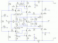
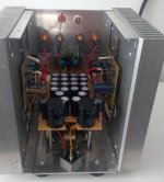
This project started few months ago when I found a nice R-core transformer in a pile of electro junk at the local flea-market (60V CT secondary, 200VA). With such a voltage/power rating the logical choice was 2 x 50W AB class amp. Lateral MOSFETs (connected as Source followers) were chosen as output devices this time too.
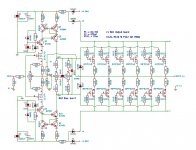
The input stage needs to provide more gain than in Cubie2 so I chose BA3-like topology with cascoded JFETs and current mirror load on them. Q5/Q8 still make a base-driven transconductance gain stage which enables GFB/NoGFB games. I chose the loop.
Vbe multiplier (Q13,R20,P1) should not be in touch with the heatsink (Laterals know how to take care of themselves), its only job is to keep the Vgs (and Id consequently) of the output stage at fixed value no matter what are the temperature/current conditions on BJTs but it can be replaced with LED or any other Vref of your choice (for Id of 200mA I need total OS Vgs of 1,3V which roughly equals the voltage drop on two 1N4148 diodes connected in series).
The current through Q1,Q2,Q9,Q12,Q3,Q6 will depend on JFETs' Idss and it can be anything from 3 to 10 mA. The current through Q4,Q5,Q7,Q8 shouldn't be higher than 4-5mA and it can be set with value of R4,R6 (the higher their value, the lower the current - and vice versa).
P1 sets the Iq in the output stage (my heatsinks can't take more than 200mA per channel comfortably, but you can go as high as your heatsinks permit you - you'll have wider cl. A regime) and the P2 sets the DC offset at the output - start adjusting with both pots at half of their value.
The gain of the amp is about 23dB, but it can be altered by simmetricaly changing the R13/R14 and R11/R22. C1,C2 will allow for about 100kHz bandwidth.
Signal-ground and power-ground are led to star-ground by separate wires.
Final result sounded good enough to retire the excellent Cubie2 (all the finesse is stil there but Cubie3 wins when it gets loud).
Attachments
Nice, so an AB beating the Cubie2?! Allthough I don't believe I need the extra watts, it certainly is the amp I have been looking for! Girlfriend is not going to be very happy, my Cubie2 is barely finalised... it will be more an end of the year project with some luck.
I do like what you did for the offset regulation with P2, can I do this too? (replace R12 =120ohm in Cubie2 by maybe 100ohm + trimmer) The layout of my PCB already forsees fixed resistor at the sources of 2SK170/SJ74, not yet used (as I do not like so much the trimmer in the feedback loop). A correction concerning my Cubie2: it is actually running at 860mA /channel @ +/-19V so in the end it is in total a little 65W stove.
http://www.diyaudio.com/forums/pass-labs/271543-cubie2-8.html#post4350695
Hi Berny,Nice, so an AB beating the Cubie2?!
yes, on loud passages with less efficient speakers, i can tell the difference.
Then there is no reason to change anything. As far as I remember, you have rather very efficient speakers...Although I don't believe I need the extra watts,
Sure, try 110R + 20R trimmer.I do like what you did for the offset regulation with P2, can I do this too? (replace R12 =120ohm in Cubie2 by maybe 100ohm + trimmer)
-------------------------------------------
Thanks Wengthis is what i call progress...(from cubie2 thread)
excellent juma.
")
Sure it can be further optimized. I did it so to accommodate for the existing case dimensions and heatsink holes (I'll do anything to avoid drilling, tapping and similar works)maybe the pcb layout need a better arrangement.
peace.
Hi Sam,
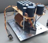
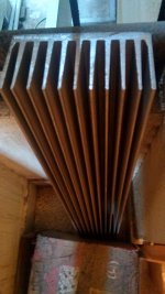
the heatsinks are not very big - 235 x 180 x 40 mm. Just about right for 20W of constant dissipation.
The datasheet says that Id_max through k1056/j162 is 7A, but I didn't hear any benefit in biasing them at more than 1A or so. You can go for higher values and see what you get...
the heatsinks are not very big - 235 x 180 x 40 mm. Just about right for 20W of constant dissipation.
The datasheet says that Id_max through k1056/j162 is 7A, but I didn't hear any benefit in biasing them at more than 1A or so. You can go for higher values and see what you get...
Hi Juma,
First, apologies for polluting your thread.
I've been playing with something similar for the last couple of months, still haven't decided on the final design - feedback, no feedback, F5 style feedback, amount etc. not enough time to play with the amp and I wouldn't rely on my memory between listening sessions.
I'm also thinking of changing the Wilson mirror to a FET type with summed triple output for more current to drive the BA2 output stage, but from what I remember, the bipolar output of the UGS was generally preferred over the FET version.
Any thoughts?
Also apologies for the poor quality image, can't get a decent resolution output from KiCad.
Attachments
Roughly, that looks similar (values I couldn't read - the pic is too small).
You plan to use heavily biased 5-pairs HEXFET output stage, so inserting the emitter follower stage before it might be a good idea (small swing loss doesn't matter since you decided on higher voltage rails for the front-end and the output stage will loose at least 9V of swing on 2 x HEXFETs' Vgs anyway). If multiple output pairs are a must, I'd rather have Laterals with small source resistors (0R1 - 0R22) - you'd loose much less swing and it would sound better (IMHO). 5 lateral pairs still can provide more than 30A_peak of output current.
You went for straight feedback loop in order to use JFETs' Source circuit for offset/harmonic structure adjustment while I chose F5-like, simmetrical feedback.
It's all OK, but only your ears will tell you what's better for you - there is no dodging that part of testing
If you can't rely on your memory only, make notes or find somebody to torture with listening sessions...

I have recently got a heatsink with one of Juma's Class A's in mind. It measures 178(W)x78(D)x900(H) and weighs about 12kgs. I am thinking of using two pieces one beside the other on each side of the chassis to get a case depth of more than 350mm. How many 'U' should I go for to try different Class A amps in the same chassis?
Attachments
The current mirrors top and bottom have the linked C to B on the multiplier side. The current through the multiplier sets the mirror currents.
Then the left side jFETs mirror that set current.
Your arrangement seems back to front from the way I understand mirrors.
But you have it working and give some current targets.
Can you explain how the current set points actually work and what the mirrors do?
Then the left side jFETs mirror that set current.
Your arrangement seems back to front from the way I understand mirrors.
But you have it working and give some current targets.
Can you explain how the current set points actually work and what the mirrors do?
Last edited:
Post #1, 4th paragraph, 1st sentence.
Current mirrors sets the currents through input branch (JFETs+cascodes) and Q5,Q8 branch to equal amount (when all current mirror emitter resistors and transistor characteristics are equal).
How the current mirror works - you'll have to do your homework and read the textbook.
Current mirrors sets the currents through input branch (JFETs+cascodes) and Q5,Q8 branch to equal amount (when all current mirror emitter resistors and transistor characteristics are equal).
How the current mirror works - you'll have to do your homework and read the textbook.

That is why I posted thisPost #1, 4th paragraph, 1st sentence.
Current mirrors sets the currents through input branch (JFETs+cascodes) and Q5,Q8 branch to equal amount (when all current mirror emitter resistors and transistor characteristics are equal).
How the current mirror works - you'll have to do your homework and read the textbook.
The current through the multiplier sets the mirror currents.
Then the left side jFETs mirror that set current.
Your arrangement seems back to front from the way I understand mirrors.
The mirror transistor that has the collector and base linked is the side that sets the mirror current.
Pull a fixed current through the shorted transistor side and the transistor on the other side (with the separated collector/base) mimics the setting current.
That was my own homework from 40years ago.
But your circuit seems to have turned this back to front. I said as much in my post.
Redoing my homework does not lead to an explanation of WHY your arrangement works with the setting of the current via the jFET side mirrors that jFET current across to the multiplier side.
You have measured the effect.
It happens.
Please explain why it works.
And you still don't get it...That was my own homework from 40years ago.
The basic function of current mirror is to copy current from one branch to another. When I, by means of degeneration, change the conditions in Iref branch (Q3) that will be reflected in other branche by changnging the current in equal amount (ideally) but in the oposite direction. Simple as that...Please explain why it works.
- Home
- Amplifiers
- Pass Labs
- Cubie3