Hi. I was licky enough to grab a set of the UGS UP Amplifier from the Swap meet a few weeks back. See the original project thread at:
http://www.diyaudio.com/forums/pass-labs/108683-ugs-power-its-u-p.html
I've being working on the project since then. I but together my own Parts Lists with the current parts and price available from Mouser and Digikey.
All pcb are almost completed. I'm waiting for the IRF240, IRF9240 matched sixtet to arrive. In the mean time I was searching for a reliable source of 2SA1209/2SC2911 used for the front end UGS cascode. These transistors are long time discontinued and I was quite worried with the full load of counterfeit from China. I'm quite happy (and relieved) to have found a reliable source in the US at a very reasonable price. There is still honest shop around, good for us Diyer")
When I got the 2SA1209/2SC2911 I measured their HFE, all looking good. Then I used my curve tracer and compare the response curves with the datasheet. Just perfect almost bang on with the specs. I then matched them by their HFE.
The top and bottom cascode are matched (Q5-Q8), same for Q9-Q12. I also matched both BC550 and BC560. Don't know if this is really necessary but it certainly couldn't hurt with such a balanced design.
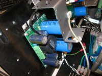
First I tested the auxiliary circuit on the main amp PCB, both front end +/-30V regs and the balanced DC output protection circuit. All were working perfectly.
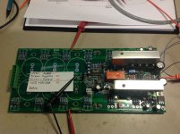
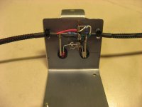
Then I installed the 2SA1209/2SC2911 on sockets for testing on the main amp pcb. I installed also sockets for the 2SK389/2SJ109 so I can matched them even closer if I experience some circuit imbalance and I couldn't adjust the output DC offset.
To be able to test the front end without the final power MOSFET, I didn't installed the VBE multiplier Q13/Q14, and used the local feedback jumper. Rout was set at 10K for testing.
With some expectation I turn on the amp channel supplies. Just great I was almost right on for the output differential and absolute DC offset, nothing was burning and the front end was working just fine I guest the close matching of all sides help in this regard.
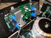
Check the picture of my test PCB. I also posted my circuit actual voltage readings. As expected all voltage readings are the same for both side of the circuit (X balanced design), hence I've shown the readings on just one side.
The specs I have so far with the Front-End only are:
Vin (BAL) = 100mv (1Khz),
Vout (SE) = 0.7V (2Vp-p), Gain: 17dB
Vout (BAL)= 1.4V (4Vp-p), Gain 23dB, (+6dB as expected, X100 specs 26dB)
BW (ref 1khz, -3dB) = 211Khz (with local feedback)
THD (1Khz) SE < 0.05%
_ _ _ _ _ _BAL < 0.005% (THD cancellation by X design, interesting...)
Noise (inputs shorted) < 0.5mv
Vin Max (BAL) = 1.9V (original X100 specs is 1.4V)
for Vout (BAL) = 26.7V
All things considered these are excellent specs
http://www.diyaudio.com/forums/pass-labs/108683-ugs-power-its-u-p.html
I've being working on the project since then. I but together my own Parts Lists with the current parts and price available from Mouser and Digikey.
All pcb are almost completed. I'm waiting for the IRF240, IRF9240 matched sixtet to arrive. In the mean time I was searching for a reliable source of 2SA1209/2SC2911 used for the front end UGS cascode. These transistors are long time discontinued and I was quite worried with the full load of counterfeit from China. I'm quite happy (and relieved) to have found a reliable source in the US at a very reasonable price. There is still honest shop around, good for us Diyer
When I got the 2SA1209/2SC2911 I measured their HFE, all looking good. Then I used my curve tracer and compare the response curves with the datasheet. Just perfect
almost bang on with the specs. I then matched them by their HFE.The top and bottom cascode are matched (Q5-Q8), same for Q9-Q12. I also matched both BC550 and BC560. Don't know if this is really necessary but it certainly couldn't hurt with such a balanced design.
First I tested the auxiliary circuit on the main amp PCB, both front end +/-30V regs and the balanced DC output protection circuit. All were working perfectly.
Then I installed the 2SA1209/2SC2911 on sockets for testing on the main amp pcb. I installed also sockets for the 2SK389/2SJ109 so I can matched them even closer if I experience some circuit imbalance and I couldn't adjust the output DC offset.
To be able to test the front end without the final power MOSFET, I didn't installed the VBE multiplier Q13/Q14, and used the local feedback jumper. Rout was set at 10K for testing.
With some expectation I turn on the amp channel supplies. Just great I was almost right on for the output differential and absolute DC offset, nothing was burning and the front end was working just fine
I guest the close matching of all sides help in this regard.Check the picture of my test PCB. I also posted my circuit actual voltage readings. As expected all voltage readings are the same for both side of the circuit (X balanced design), hence I've shown the readings on just one side.
The specs I have so far with the Front-End only are:
Vin (BAL) = 100mv (1Khz),
Vout (SE) = 0.7V (2Vp-p), Gain: 17dB
Vout (BAL)= 1.4V (4Vp-p), Gain 23dB, (+6dB as expected, X100 specs 26dB)
BW (ref 1khz, -3dB) = 211Khz (with local feedback)
THD (1Khz) SE < 0.05%
_ _ _ _ _ _BAL < 0.005% (THD cancellation by X design, interesting...)
Noise (inputs shorted) < 0.5mv
Vin Max (BAL) = 1.9V (original X100 specs is 1.4V)
for Vout (BAL) = 26.7V
All things considered these are excellent specs
Attachments
Last edited:
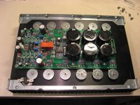
I'm resuming my UP amp story now that the amp is completed and working like a charm I new that my front end was working correctly, I tested the other channel and it was fine as well. Then I started with the chassis in order to complete the supply so i can test the final into an actual dummy load.
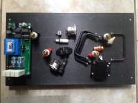
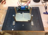
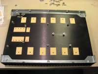
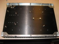
I just received the case from Hifi2000 and it is looking great. I got the 3mm panel thickness version. I started with the rear panel. First picture is showing the bare rear panel with all the parts, then the finish product after a day working in my garage workshop.
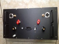
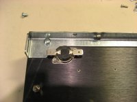
I bought a nice pair of propeller speaker terminals because they looked a little like the original Pass Labs connectors. The white binding post will be the signal gnd, to use with an external subwoofer speaker connection for example, since the Plus/Minus of the speaker are not referenced to ground.
Main power on is using a breaker. There will be a power on switch on the front to control the softstart pcb.
Small hole on the bottom is for the remote power-on, again a feature built-in the softstart pcb
I new that my front end was working correctly, I tested the other channel and it was fine as well. Then I started with the chassis in order to complete the supply so i can test the final into an actual dummy load.I just received the case from Hifi2000 and it is looking great. I got the 3mm panel thickness version. I started with the rear panel. First picture is showing the bare rear panel with all the parts, then the finish product after a day working in my garage workshop.
I bought a nice pair of propeller speaker terminals because they looked a little like the original Pass Labs connectors. The white binding post will be the signal gnd, to use with an external subwoofer speaker connection for example, since the Plus/Minus of the speaker are not referenced to ground.
Main power on is using a breaker. There will be a power on switch on the front to control the softstart pcb.
Small hole on the bottom is for the remote power-on, again a feature built-in the softstart pcb
Attachments
Last edited:
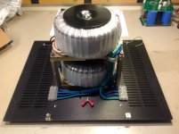
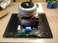
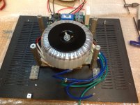
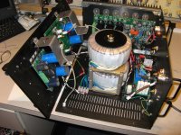
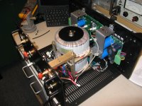
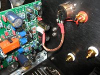
Then the bottom plate assembly for the softstart PCB and the pair of power transformers. I really like what I did with the transformers. The case I choose is higher than deeper. I couldn't put both transformers side by side, then I had to mount them over each other. Both transformers, one per channel so the amp is really a true dual mono design are 400VA each, for a total of 800VA.
Again as I often do, I recycled very nice machines aluminum plates from a GOES transmitter. These plates are strong, leveled and easy to drill. I reused the mounting threaded holes of the bottom's one to screw it to the amp bottom plate. I used large standoffs (again recycled) to space both plates. The second picture from the left (see the red arrow) is showing some vibration damping foam (from a Furutech ac outline packaging) that I recycled and put there just in case.
The transformers primaries are connected using a vertically mounted screw strip terminal. Using jumpers I can easily configure them to 117V or 234V line voltage.
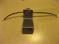
The 4th pictureis showing the Power-On/SoftStart CPB mounted on the back. The PCB is slightly modified by me. First the small power transformer can now be selected from 110 or 220V primaries. Then the DC supply voltage was a little too high (we have 120V in Canada, not 110V), I added a small 3 pins LM317 pre-regulator before the rest of the PCB supplies 12V regs circuit. Then I added a connection to put in series the thermal cutoff switch that will be mounted on each channel heatsink for 75C cutoff protection. If on of the switch opens over 75V, that will remove the pre 12V reg voltage, shutting down the amp. The small screw terminal I added on the right is to connect in series both 75C NC switches. If not used simply put a shorting jumper in there. Finally the case safety ground in on the left.
Since the transformers secondaries wires were too big for the UP rectifier PCB terminals, I terminated then into screw terminals on the bottom plate. This way I can easily disconnect the transformers from the rectifiers that will be mounted on the amp front plate for cooling.
It is looking rather nice I think The mounting plates also add to the bottom plate rigidity.
Again as I often do, I recycled very nice machines aluminum plates from a GOES transmitter. These plates are strong, leveled and easy to drill. I reused the mounting threaded holes of the bottom's one to screw it to the amp bottom plate. I used large standoffs (again recycled) to space both plates. The second picture from the left (see the red arrow) is showing some vibration damping foam (from a Furutech ac outline packaging) that I recycled and put there just in case.
The transformers primaries are connected using a vertically mounted screw strip terminal. Using jumpers I can easily configure them to 117V or 234V line voltage.
The 4th pictureis showing the Power-On/SoftStart CPB mounted on the back. The PCB is slightly modified by me. First the small power transformer can now be selected from 110 or 220V primaries. Then the DC supply voltage was a little too high (we have 120V in Canada, not 110V), I added a small 3 pins LM317 pre-regulator before the rest of the PCB supplies 12V regs circuit. Then I added a connection to put in series the thermal cutoff switch that will be mounted on each channel heatsink for 75C cutoff protection. If on of the switch opens over 75V, that will remove the pre 12V reg voltage, shutting down the amp. The small screw terminal I added on the right is to connect in series both 75C NC switches. If not used simply put a shorting jumper in there. Finally the case safety ground in on the left.
Since the transformers secondaries wires were too big for the UP rectifier PCB terminals, I terminated then into screw terminals on the bottom plate. This way I can easily disconnect the transformers from the rectifiers that will be mounted on the amp front plate for cooling.
It is looking rather nice I think
The mounting plates also add to the bottom plate rigidity.Attachments
Last edited:
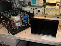
Then I mounted the two rectifiers, first part of the CLC filter (last part been all the caps mounted on each output section pcb) and voltage doubler (to supply the front end) on the 10mm front panel to act as a heatsink for the diodes.
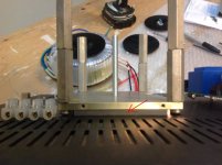
The chassis is mainly two plates (front and back) and the two side heatsinks. In order to test/adjust each channel module, the front and the back need to be kept in place without the normally mounted sides.
In order to do that I built custom aluminum brackets to connect the front to the center transformer assy insuring a stable mounting point in absence of the sides.
The images are showing the rectifier pcb and the brackets. The front panel boards can be tested in place since the front can rest ont the front handle at an angle, and I have enough place to take measurement or to do the assy and connections.
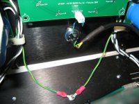
Each supply ground is elevated from the chassis ground by CL-60 thermistor to eliminate current loop. The lift ground is connected on the chassis on one point.
Last picture on the right is showing the rectifier supply from the transformer secondary, mounted on the chassis bottom plate.
The chassis is mainly two plates (front and back) and the two side heatsinks. In order to test/adjust each channel module, the front and the back need to be kept in place without the normally mounted sides.
In order to do that I built custom aluminum brackets to connect the front to the center transformer assy insuring a stable mounting point in absence of the sides.
The images are showing the rectifier pcb and the brackets. The front panel boards can be tested in place since the front can rest ont the front handle at an angle, and I have enough place to take measurement or to do the assy and connections.
Each supply ground is elevated from the chassis ground by CL-60 thermistor to eliminate current loop. The lift ground is connected on the chassis on one point.
Last picture on the right is showing the rectifier supply from the transformer secondary, mounted on the chassis bottom plate.
Attachments
Last edited:
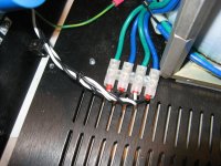
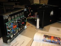
Same thing with the rear panel, here again a bracket to hold the back in place without the side. Since I had two bracket on the front, and that one of the rectifier pcb meter output supplies connector was not used, I decided to installed leds on them. These leds light the inside in red & blue to get a look a liitle like the Chords amps. Everything is mounted point-to-point with quick disconnect connectors.
Attachments
Then finally the output section., one channel per heatsink. I started with the the bare heatsink, used the pcb drill pattern to mark all the holes, drilled and tap. I used blind hole tap hence I didn't have to drill the holes all the way.
I installed the 75C cutoff protection, the PCB standoff, the multiple insulation pads, and mounted the PCB. Finally I tested all transistors to insure none of them was shorting to the heatsink.
The PCB is positioned to insure that the input and the power supply wires are short. The input wires are cardas, with furutech recycled copper shielding.
Attachments
Last edited:
Ok, thanks.
...Check Toroidy.pl ....this amp deserves good trafos...they will get you exactly what you need.
- Status
- This old topic is closed. If you want to reopen this topic, contact a moderator using the "Report Post" button.
- Home
- Amplifiers
- Pass Labs
- My UGS UP Amplifier