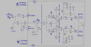
Class aP Signal-Tracking Bipolar [PSU] using LM317T and LM337T
Please find two attached pictures of the subject prototype.
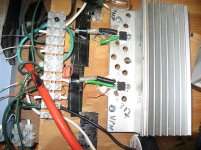
1. The left picture shows LM317T and LM337T affixed to a heat sink. The upper [LM337T] is shown to have its power output loaded with a light bulb [5W]; like that of the lower LM317T [not visible].
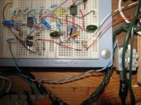
2. The right picture shows the OpAmp control circuits for their schematic of the previous post; which is also attached.
3. The tracking PSU is DC coupled throughout. No capacitors and inductors are allowed [in series with or in parallel to] elements in the control [OpAmps] and power output circuits. They will degrade the intrinsic slew-rate [rise and fall] of the analog pulses. Thus defeating this Class aP approach and rendering it useless for PSU tracking olf the music signal.
3a. Point 3 above is emphasized as follows. I did not use capacitors at the output of the voltage regulators as recommended by their maker to improve/enhance their stability. I also did not use film bypass capacitors [e.g. 0.1 uF] at the voltage-variable rails of the front end buffer [LF356N].
4. The loads to this bipolar voltage-variable PSU is explained as follows for a generic complementary symmetry BJT power out stage which is powering a loudspeaker.
4a. The positive voltage-variable power output of LM317T goes to the collector of NPN [load] of the example music power output stage in point 4.
4b. The negative voltage-variable power output of LM337T goes to collector of PNP [load] of the example music power output stage stage in point 4.
4c. I'd be pleasantly surprised if all of an actual music power amp [meaning by example its front end diff amp plus its last voltage amp plus its output current drivers and its power output stage] are driven by this bipolar voltage-variable PSU like that shown in the attached schematic for the front end target buffer [LF356N]. Note that an earlier circuit showed the idle PSU of LF356N at ~+/-3Vdc. The operation of this wishful-music amp is thus likened to that of an accordion.
Best
Anton
Please find two attached pictures of the subject prototype.
1. The left picture shows LM317T and LM337T affixed to a heat sink. The upper [LM337T] is shown to have its power output loaded with a light bulb [5W]; like that of the lower LM317T [not visible].
2. The right picture shows the OpAmp control circuits for their schematic of the previous post; which is also attached.
3. The tracking PSU is DC coupled throughout. No capacitors and inductors are allowed [in series with or in parallel to] elements in the control [OpAmps] and power output circuits. They will degrade the intrinsic slew-rate [rise and fall] of the analog pulses. Thus defeating this Class aP approach and rendering it useless for PSU tracking olf the music signal.
3a. Point 3 above is emphasized as follows. I did not use capacitors at the output of the voltage regulators as recommended by their maker to improve/enhance their stability. I also did not use film bypass capacitors [e.g. 0.1 uF] at the voltage-variable rails of the front end buffer [LF356N].
4. The loads to this bipolar voltage-variable PSU is explained as follows for a generic complementary symmetry BJT power out stage which is powering a loudspeaker.
4a. The positive voltage-variable power output of LM317T goes to the collector of NPN [load] of the example music power output stage in point 4.
4b. The negative voltage-variable power output of LM337T goes to collector of PNP [load] of the example music power output stage stage in point 4.
4c. I'd be pleasantly surprised if all of an actual music power amp [meaning by example its front end diff amp plus its last voltage amp plus its output current drivers and its power output stage] are driven by this bipolar voltage-variable PSU like that shown in the attached schematic for the front end target buffer [LF356N]. Note that an earlier circuit showed the idle PSU of LF356N at ~+/-3Vdc. The operation of this wishful-music amp is thus likened to that of an accordion.
Best
Anton
Attachments
A DEF-Style Amp using a Class aP signal-tracking bipolar PSU
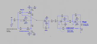
I showed a DEF-Style amp using LM317T [as a pseudo-Depletion device] and TIP125 [as Enhancement BJT] in post #286 of the thread "DEF Amp" by Mr. Pass. It used a fixed +/-17.5 Vdc PSU and it inverted the phase of its input signal. Please review therein its details of operation.
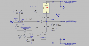
The attached schematic is for a prototype amp which is the target of a Class aP signal-tracking bipolar PSU. It does not invert the phase of its input signal. Its idle PSU rails are +/-7 Vdc, and each device is biased at 100 mA. Please note the following definitions and details:
1. Signal-tracking means that both PSU rails of the DEF-Style amp follow its power output voltage signal.
2. The positive-going [+7Vdc] rail means this idle power voltage moves towards [+15 Vdc] under the influence of the analog pulse riding atop of it.
3. The negative-going [-7Vdc] rail means this idle power voltage moves towards [-15 Vdc] under the influence of the analog pulse riding atop of it.
4. I used a deluxe and a stiff cascoded constant current source [4.46 mA] to properly bias LM317T. It locks its [Vadj-Vout] at -1.245 Vdc. This specific voltage did not vary with the excitation music signal.
5. A Zobel at its power output decreases high frequency noise.
6. A capacitor [18 pF] between the output of OPA134 and its inverting input cured an output oscillation.
7. The voltage gain of the amp is +2.8 from the equation: [1 + (10K/5.6K)]. Its music source is the volume-controlled headphone output of a Marantz CD player.
8. This amp drives an ADS L730 [3-way] loudspeaker. Its rated impedance is 6 Ohms and may dip to 4 Ohms.
9. This amp has a useful and a maximum [5 Vp-p] across said loudspeaker. It is stable against oscillation and sounds great. The sound is open and airy.
The next post will show the complete schematic for this amp plus its voltage-variable bipolar PSU.
Best
Anton
I showed a DEF-Style amp using LM317T [as a pseudo-Depletion device] and TIP125 [as Enhancement BJT] in post #286 of the thread "DEF Amp" by Mr. Pass. It used a fixed +/-17.5 Vdc PSU and it inverted the phase of its input signal. Please review therein its details of operation.
The attached schematic is for a prototype amp which is the target of a Class aP signal-tracking bipolar PSU. It does not invert the phase of its input signal. Its idle PSU rails are +/-7 Vdc, and each device is biased at 100 mA. Please note the following definitions and details:
1. Signal-tracking means that both PSU rails of the DEF-Style amp follow its power output voltage signal.
2. The positive-going [+7Vdc] rail means this idle power voltage moves towards [+15 Vdc] under the influence of the analog pulse riding atop of it.
3. The negative-going [-7Vdc] rail means this idle power voltage moves towards [-15 Vdc] under the influence of the analog pulse riding atop of it.
4. I used a deluxe and a stiff cascoded constant current source [4.46 mA] to properly bias LM317T. It locks its [Vadj-Vout] at -1.245 Vdc. This specific voltage did not vary with the excitation music signal.
5. A Zobel at its power output decreases high frequency noise.
6. A capacitor [18 pF] between the output of OPA134 and its inverting input cured an output oscillation.
7. The voltage gain of the amp is +2.8 from the equation: [1 + (10K/5.6K)]. Its music source is the volume-controlled headphone output of a Marantz CD player.
8. This amp drives an ADS L730 [3-way] loudspeaker. Its rated impedance is 6 Ohms and may dip to 4 Ohms.
9. This amp has a useful and a maximum [5 Vp-p] across said loudspeaker. It is stable against oscillation and sounds great. The sound is open and airy.
The next post will show the complete schematic for this amp plus its voltage-variable bipolar PSU.
Best
Anton
Attachments
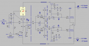
DEF-Style amp using a Class aP signal-tracking bipolar PSU
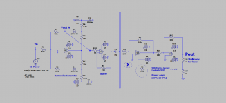
The attached complete schematic is for the subject prototype power amp. Please note the following:
1. The sub-schematic to the left of the star vertical boundary is the DEF-Style power amp. I discussed its operation in the previous post. I chose to operate it at a voltage gain equal to 1. It is the recipient of the real-time bipolar PSU which tracks its power output voltage across a 4 Ohm load.
2. The power output of the DEF-Style amp also feeds the input of the following Precision Rectifier [PR]. It is sandwiched between the star and $-signs vertical barriers. I also discussed its operation in earlier posts. Note its input signal is 20 KHz at an amplitude of 12 Vp-p.
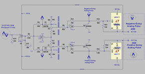
3. To the right of of the $-signs vertical barrier is the power output of the bipolar PSU.
3a. Consider the upper OpAmp [U2] as the working example. Its inverting port sums a reference voltage [+6.1Vdc from its LED circuit] with a positive- going analog pulse timed from t to t1 seconds.
3b. The output of OpAmp [U2] sits at [-6.1 Vdc] fixed voltage atop which rides the negative-going analog pulse.
3c. This output of [U2] is presented to the base of power PNP which operates as a follower [buffer]. PNP has a high Hfe [90 to 180]. It is is easily driven by the Op Amp.
3d. The emitter of power PNP is the real-time and voltage variable negative rail for the DEF-Style amp. It feed the collectors of its TIP125 BJT.
4. The lower OpAmp [U3] and its power NPN buffer generates the real-time and voltage-variable positive rail for the DEF-Style amp. The positive rail of the DEF-Style amp is the input port of LM317T.
5. Signal timing [0 to t and t to t1 seconds] is most important for the proper operation of the amp. This is the [coincident timing] of the AC and its analog pulse signals.
I'll stop here and follow-up in the next post on the value of this approach which is simple, stable and expected to be adaptable to high power systems. I also have photos of the prototype.
Best wishes
Anton
The attached complete schematic is for the subject prototype power amp. Please note the following:
1. The sub-schematic to the left of the star vertical boundary is the DEF-Style power amp. I discussed its operation in the previous post. I chose to operate it at a voltage gain equal to 1. It is the recipient of the real-time bipolar PSU which tracks its power output voltage across a 4 Ohm load.
2. The power output of the DEF-Style amp also feeds the input of the following Precision Rectifier [PR]. It is sandwiched between the star and $-signs vertical barriers. I also discussed its operation in earlier posts. Note its input signal is 20 KHz at an amplitude of 12 Vp-p.
3. To the right of of the $-signs vertical barrier is the power output of the bipolar PSU.
3a. Consider the upper OpAmp [U2] as the working example. Its inverting port sums a reference voltage [+6.1Vdc from its LED circuit] with a positive- going analog pulse timed from t to t1 seconds.
3b. The output of OpAmp [U2] sits at [-6.1 Vdc] fixed voltage atop which rides the negative-going analog pulse.
3c. This output of [U2] is presented to the base of power PNP which operates as a follower [buffer]. PNP has a high Hfe [90 to 180]. It is is easily driven by the Op Amp.
3d. The emitter of power PNP is the real-time and voltage variable negative rail for the DEF-Style amp. It feed the collectors of its TIP125 BJT.
4. The lower OpAmp [U3] and its power NPN buffer generates the real-time and voltage-variable positive rail for the DEF-Style amp. The positive rail of the DEF-Style amp is the input port of LM317T.
5. Signal timing [0 to t and t to t1 seconds] is most important for the proper operation of the amp. This is the [coincident timing] of the AC and its analog pulse signals.
I'll stop here and follow-up in the next post on the value of this approach which is simple, stable and expected to be adaptable to high power systems. I also have photos of the prototype.
Best wishes
Anton
Attachments
The suggested amp has this dual value:
1. It partitions overall heat dissipation such that the power output stage of the DEF-Style amp dissipates the least heat [1.1 W at idle]. The power buffer BJTs dissipate the rest of the designed heat. And the extent of this dissipation [in BJTs] is solely a function of the magnitude of their Vce value at idle [20 V] and under dynamic operation.
2. The DEF-style power output stage operates in a pseudo-cascode mode as was described earlier. The values of its components' Vce are held constant at 5.5Vdc during operation.
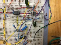
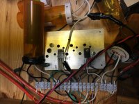
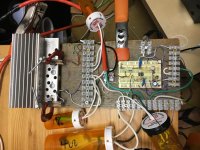
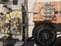
The left picture is for the DEF-Style power amp. It is commensurate with its aforementioned schematic. Most important is to have a star ground because of the large currents which are processed, and it is a sanitary electrical practice. This star ground is the white EU-style connector at the bottom of the pic. The heat sink barely warms up in operation; meaning while it delivers a 12Vp-p signal [20 KHz.] across a 4 Ohm power resistor.
The middle picture is for the complementary symmetry power buffer BJTs on their heat sink. Their emitters are the source of the bipolar and high current PSU driving the DEF-Style amp. Their heat sink warms up during the aforementioned operation at 20 KHz.
The right picture is for the Precision Rectifier [PR; bottom chip], and the power BJT buffer drivers [2 Op Amps on the top side]. The dark single wire at the right side carries the signal [to be tracked] from the output of the DEF-Style amp to the input of [PR].
The parts of this amp are spread out. This [loose layout] did not cause oscillation or foul operation.
I analyze operation of the Class aP voltage-variable PSU on the scope while playing music. The analog pulses [at the emitter of the Power Buffer BJTs] must be clean and they are. No fuzz riding on them; meaning spurious oscillation during bass and treble transients.
It did not matter to operation whether the signal to be tracked emanated from the power output [Vout] or the input [Vin] of the DEF-Style amp. Both approaches gave a fast real-time operation.
This is a good news alternate approach of feed forward instead of fold back [retro] the rails of the Class aP voltage-variable PSU. The operation of all of the building blocks therein the totality of this amp are linear. They are governed by simple linear [algebraic] equations. Since I know [or can readily measure] the voltage gain of each block [e.g. that of PR, DEF-Style amp etc..], I can calculate the other needed values of gain in the circuit chain. Thus I can determine the desired and must needed pseudo-cascode operation of the output stage for any power amp.
I am not sure what Power Supply Rejection [PSR] means for this amp!
Best
Anton
1. It partitions overall heat dissipation such that the power output stage of the DEF-Style amp dissipates the least heat [1.1 W at idle]. The power buffer BJTs dissipate the rest of the designed heat. And the extent of this dissipation [in BJTs] is solely a function of the magnitude of their Vce value at idle [20 V] and under dynamic operation.
2. The DEF-style power output stage operates in a pseudo-cascode mode as was described earlier. The values of its components' Vce are held constant at 5.5Vdc during operation.
The left picture is for the DEF-Style power amp. It is commensurate with its aforementioned schematic. Most important is to have a star ground because of the large currents which are processed, and it is a sanitary electrical practice. This star ground is the white EU-style connector at the bottom of the pic. The heat sink barely warms up in operation; meaning while it delivers a 12Vp-p signal [20 KHz.] across a 4 Ohm power resistor.
The middle picture is for the complementary symmetry power buffer BJTs on their heat sink. Their emitters are the source of the bipolar and high current PSU driving the DEF-Style amp. Their heat sink warms up during the aforementioned operation at 20 KHz.
The right picture is for the Precision Rectifier [PR; bottom chip], and the power BJT buffer drivers [2 Op Amps on the top side]. The dark single wire at the right side carries the signal [to be tracked] from the output of the DEF-Style amp to the input of [PR].
The parts of this amp are spread out. This [loose layout] did not cause oscillation or foul operation.
I analyze operation of the Class aP voltage-variable PSU on the scope while playing music. The analog pulses [at the emitter of the Power Buffer BJTs] must be clean and they are. No fuzz riding on them; meaning spurious oscillation during bass and treble transients.
It did not matter to operation whether the signal to be tracked emanated from the power output [Vout] or the input [Vin] of the DEF-Style amp. Both approaches gave a fast real-time operation.
This is a good news alternate approach of feed forward instead of fold back [retro] the rails of the Class aP voltage-variable PSU. The operation of all of the building blocks therein the totality of this amp are linear. They are governed by simple linear [algebraic] equations. Since I know [or can readily measure] the voltage gain of each block [e.g. that of PR, DEF-Style amp etc..], I can calculate the other needed values of gain in the circuit chain. Thus I can determine the desired and must needed pseudo-cascode operation of the output stage for any power amp.
I am not sure what Power Supply Rejection [PSR] means for this amp!
Best
Anton
Attachments
A DEF amp using a signal-tracking bipolar PSU
Dennis Hui quotes Mr. Pass at the bottom of his posts as follows: "We are fearless amplifier builders. A little heat doesn't scare us at all.- NP 2002"
I can't escape "heat generation" in Pass-style amplifiers; who does? But the subject approach allows me to partition this generous heat between the music processor [DEF] and its PSU. For added fun, it further allows one to study the effect of its heat content; aka enthalpy [or its temperature at set bias] on performance.
The attached schematic is for the subject prototype DEF amp. The DEF circuit therein is to the left of the *-sign vertical barrier. This amplifier sounds great and is stable like I've known DEF to be. It idles at +/-0.2 A. This suggests a Class A/B amp
DEF generates very little heat; ~1W per FET at idle. The remaining heat load is carried by the Class aP signal-tracking bipolar PSU; specifically its complementary BJT power followers. I must emphasize that the system's [DEF and PSU] "overall size of its heat sink" is at a minimum equal to or most probably larger than that for a reference Pass DEF amp using a classical Pass PSU. No escaping that!
The content of my earlier posts on this subject fully applies here. I'll add remnant thoughts in a future post.
Best
Anton
Attachments
good work ..... it seems you have all the fun you need")
Thanks ZM. This fanatic fun will not end. This PSU approach may be useful to soft-start power output stages which use depletion devices.
Best
Anton
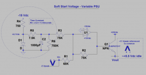
A Concept Class aP Soft-Start Voltage-Variable PSU.
I am vigilant when I experiment with a Normally-ON power FET; especially since it makes great sounding amps, it is fun to work with, and can become extinct and/or unobtainium.
The attached schematic is shown as an example for only the positive voltage variable circuit PSU of the prototype DEF amp understudy. The negative side of its PSU is configured exactly like it; but with polarity reversal of the relevant components and signals therein etc.
Here is the envisioned sequence of operation for the totality of this DEF amplifier. The loudspeaker load is connected:
1. The sole and main high power PSU [e.g. +/-25 Vdc] is turned on at the amp's AC power switch.
2. The power rail voltages of this main PSU reach steady state.
3. The resultant negative rail [-25Vdc] of the main PSU is the voltage needed to bias the DEF FETs via the resistor ladder which is shown in the schematic.
4. A reference +/- 15 Vdc PSU source is simultaneously derived from the main +/-25 Vdc PSU so as to power the Op Amps and the Soft-Start circuit.
5. The encircled Soft-Start circuit uses the established concept of Time Constant for its operation.
6. The indicated time-constant of ~7.5 second is an example. It is adjustable and needs to be measured to be safe and sure.
7. The output voltage at the capacitor of the "time constant" circuit starts at zero Vdc. This negative-going voltage ramps up as predicted and at [~-0.5 Vdc] the power NPN turns on and its base tracks this positive-going ramp voltage.
8. The above suggests that a sufficient length of time will elapse which enables the priority biasing of the DEF FETs. And further starts off the DEF's bipolar power rails at close to zero Vdc.
9. At long time the Time Constant circuit reaches steady steady. The voltage on the timing capacitor reaches ~-6.2 Vdc.
10. On AC power turn-off, the resistor [750 K] discharges the timing capacitor.
Best
Anton
Attachments
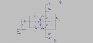
Generator of even and odd harmonics.
The H2 circuit [and thread] by Mr. Pass have generated a good "buzz; from said harmonics!" in this forum. The attached schematic is that of a Precision Rectifier which I've discussed at length in past posts. In this post, it is a model circuit which was manipulated in LTSpice. The resultant FFT signature of signals in this circuit is like that of H2 by Mr. Pass. Please note:
1. The encircled feedback resistors [90K and 100K] cause an imbalance in amplification. Their different values are responsible for birthing H2..
2. There is a certain phase [either positive or negative, unknown here] which is due to the location of the feedback resistors.
3. Swap the location of the feedback resistors in the shown circuit. The other phase of H2 is expected to emerge.
4. The fundamental frequency [1KHz] plus the harmonics emerge at the output of the OpAmp [Vout]. This is unlike generating analog pulses.
5. Pay attention to the "looks" of the signal at the inverting input of the OpAmp. It must be a sine wave.
Best
Anton
Attachments
Since R1 and R2 form a voltage divider you could replace them with a 200K potentiometer and give the human user a front panel knob to play with. "Tunefulness" might be one possible label for the pot.
Great idea and label. Thanks. The wiper of the pot will connect to the inverting input of the OpAmp.
Another Headphone Amp...
Except that I deliberately infused its power output signal with mostly the second harmonic distortion [H2]. Mostly; means absent odd order harmonics; per the FFT output of the attached Spice XVII file.
The input stage of the headphone amp [HA] is shown in the attached schematic. It is a modified analog pulse precision rectifier. Vout A and Vout B are the relevant output signals [fundamental frequencies] which are infused with H2. The signal at Vout C is totally void of H2.
Note the magnitude of the simulation input signal [Vin] which is 100 mV rms. I've already assembled HA and listened to it using Vout B. The actual CD player's [Vin] was monitored by the scope. It runs ~20 mVp-p. Its magnitude can be used to throttle the magnitude of H2.
I'll show the complete schematic of HA in the upcoming post.
Best
Anton
Attachments
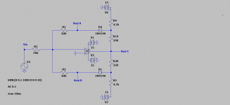
A model headphone amp
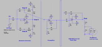
The attached schematic shows one channel of a model headphone amp [HA].
2nd order harmonics generator [H2].
Its schematic is to the left of the single-line vertical barrier. It was shown in the previous post. Please note:
1. The music generator is a SONY CD player. It has a [handy] motorized remote volume control. In application, the output signal at [Vout A, or B or C] was adjusted to an average of ~ 20 mVp-p.
2. Vout C of the generator is void of H2 [via FFT] and is essentially the fundamental frequency.
3. Vout A and Vout B show [via FFT] the fundamental frequency plus H2. Since Vout C is the center point of Vout A and Vout B, it follows that the [important] phase of H2 at Vout A is opposite to or is out of phase with that at Vout B. Thus, two independent phases of H2 relative to the phase of the partner fundamental are generated. A total of six [Vout A, B, C] combinations are present when on flips the overall phase at the output signal of the power amp.
4. The subjective performance of the signals at Vout A, B and C are readily discernible per the teaching of Mr. Pass in his article "H2 Harmonic Generator". Vout C didn't care when the relative phase at the headphones was flipped.
5. The magnitude of H2 [distortion] relative to its fundamental is controlled by the SONY volume control. Higher input signals from the SONY [ say from 20 mVp-p to 30 mVp-p] is expected to give more distortion.
Preamplifier
It buffers the signals at Vout A or Vout B. It has an adjustable non-inverting gain of 2.5.
THRESHOLD S/150 Power Amp.
It has a non-inverting voltage gain of ~21. The gain of the preamplifier and that of THRESHOLD S/150 establish the required voltage the headphones need to be driven to a comfortable and safe listening level. This input voltage to each phone averages at ~ 100 mVp-p for the GRADO Labs Prestige Series.
The load to S/150 is 5 Ohms and is configured as a voltage divider [4 plus 1 in series]. Both phones are connected in parallel and were driven from the voltage across the grounded 1 Ohm power resistor.
It works. Its subjective performance from the choice of [ Vout A or B or C] is different and is fully agreeable/pleasing.
Best
Anton
Attachments
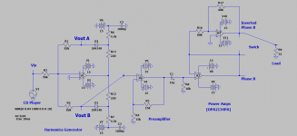
A Stereo Headphone Amp [HA 1] Imbibed with H2
The schematic for one channel of the subject, and a picture of its prototype are attached. Please focus on the schematic:
1. It has a front-end harmonic generator [H2]. It is followed by a non-inverting buffer of voltage gain = 2. This buffer drives the power output stages.
2. The power output stages is an OPA2134PA OpAmp. One power output channel is non-inverting while the other inverts phase. It allows you to choose phase to the headphones load on the fly; so as to select the sound you like. This schematic shows the Inverted Phase B I like.
3. My hearing need of Grado Headphones is a voltage drive per phone of ~ 50 mVp-p to an absolute 100 mVp-p maximum [for a headache]. The OpAmp is fully capable to supply a maximum ~ 3 mAp-p.
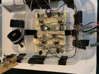
Please focus on the picture of the prototype. It is a stereo headphone power amp:
1. It has two joined prototype boards. Each chip on the bottom board [OPA2134PA] is a harmonic generator and is mated with its non-inverting buffer of voltage gain =2.
2. Each chip [OPA2134PA] on the upper board is the two power output stages per channel; a non-inverting and an inverting buffers of equal voltage outputs [for A/B comparison on the fly]. The white wire [R channel] and the violet wire [L Channel] are moved at will from their shown position of [Inverted Phase B] to the ones [ Phase B] below them while the music plays.
* The phase [inverted Phase B] I liked may suggest I was hearing the music fundamentals which are imbibed with their negative phase H2. The resultant sound field is spacious, kind and outside my head. The other [Phase B] put the music mostly in my head.
I will need to understand the phase of H2 at [Vout A] compared with that at [Vout B] in the harmonic generator by using the same setup.
Best
Anton
The schematic for one channel of the subject, and a picture of its prototype are attached. Please focus on the schematic:
1. It has a front-end harmonic generator [H2]. It is followed by a non-inverting buffer of voltage gain = 2. This buffer drives the power output stages.
2. The power output stages is an OPA2134PA OpAmp. One power output channel is non-inverting while the other inverts phase. It allows you to choose phase to the headphones load on the fly; so as to select the sound you like. This schematic shows the Inverted Phase B I like.
3. My hearing need of Grado Headphones is a voltage drive per phone of ~ 50 mVp-p to an absolute 100 mVp-p maximum [for a headache]. The OpAmp is fully capable to supply a maximum ~ 3 mAp-p.
Please focus on the picture of the prototype. It is a stereo headphone power amp:
1. It has two joined prototype boards. Each chip on the bottom board [OPA2134PA] is a harmonic generator and is mated with its non-inverting buffer of voltage gain =2.
2. Each chip [OPA2134PA] on the upper board is the two power output stages per channel; a non-inverting and an inverting buffers of equal voltage outputs [for A/B comparison on the fly]. The white wire [R channel] and the violet wire [L Channel] are moved at will from their shown position of [Inverted Phase B] to the ones [ Phase B] below them while the music plays.
* The phase [inverted Phase B] I liked may suggest I was hearing the music fundamentals which are imbibed with their negative phase H2. The resultant sound field is spacious, kind and outside my head. The other [Phase B] put the music mostly in my head.
I will need to understand the phase of H2 at [Vout A] compared with that at [Vout B] in the harmonic generator by using the same setup.
Best
Anton
Attachments
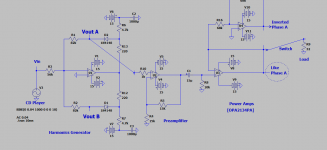
Another simpler option.
I used the attached schematic to study the subjective performance of the alternate signal source [Vout A] in the harmonic generator instead of [Vout B].
I liked [Phase A] which was presented to the headphones. It was not inverted like that [in previous post] which I liked emanating from [Vout B]. I now can get rid off one OPA2134PA and thus simplify the prototype..
It follows that the harmonic generator yielded:
1. Fundamental music frequencies which are impregnated with negative phase H2 at [Vout A].
2. Fundamental music frequencies which are imbibed with positive phase H2 at [Vout B].
Ideas for the power output stages in the event OpAmps are not preferred
1. Use the front end of BA3 [BA3 FE] to process the music signals emanating from [Vout A]. It does not invert phase and is expected to have a voltage gain of 3 when using a 32 Ohm phone. But note that this is a current source amp; unlike the voltage source OPA2134PA OpAmp. I would DC-servo its output to get rid of its coupling cap, and maybe eliminate the pot at the sources of the JFETs.
2. Use Juma's LSK- BAF...pre/line amp to process music signals emanating [from Vout B]; because it inverts phase.
Best
Anton
Attachments
Thanks Mark Johnson for the link. I fully agree. This chip has an impressive cost/unity gain performance.Mouser is now selling the surface mount BUF634A for less than three dollars link
Output current is 250mA, supply voltage max is +/- 18V, GBWP is 200 MHz, Slew Rate is 3.7 volts per nanosecond.
It might be an inexpensive way to drive headphones.
~
The attached schematic is for a prototype headphone amp whereby:
1. The fundamental music signals are first imbibed with H2 [negative phase; -50dB] as described in earlier posts..
2. The power amp [OPA2134] driving the headphones then adds Positive Current Feedback [PCF] to the resultant music signal above. Its circuit is shown to the right side of the double line vertical barrier.
3. This power amp is comprised of 2 OpAmp inverters [OPA2134PA] which are connected in series. This setup allows for the inclusion of [PCF].
One must separate the common ground of the headphones into two; so as to enable an independent [PCF] for each phone or earbud.
The separation of the common ground lead was done to a Panasonic XBS headphone [25 Ohm], and to a Skullcandy earbuds [16 Ohm]. I was able to listen to each transducer for ~1 hour with little fatigue.
The minimum value of the [PCF] encircled resistor [15 K] is 1.2 K. The simulation showed oscillation at a value of 1 K.
Best
Anton
Attachments
Audio System for Headphones
Mr. Pass taught audio DIYers the musical value of Positive Current Feedback [PCF] in F7, and that of imbibing the music's fundamental signals with their negative phase second harmonics [H2np].
The headphone amp [HA] prototype in this post is one of a kind. It utilizes both PCF and H2np [unlike any HA out there]; so as to express their established sonic enhancements during one's music's headphone experience. And it does/delivers for my ears!
The attachments show a picture of the prototype. I cut the plug to Grado headphones so as to separate their common return lines [blue] as shown in the picture. This was needed to use [PCF] in the power output stage of each stereo channel.
I have shown you this schematic in past posts. Note the encircled [1.5 K] resistor in the path of [PCF]. This low valued feedback resistor gave a high extent of [PCF]. This audio system is stable against oscillation, noiseless and a pleasure to listen to.
Best
Anton
Attachments
Headphone Amp-H2nPCF
I have attached a picture of the prototype headphone amp [PHA] and its final schematic. I noticed a [+5 mV] and a [+25 mV ] DC offset at the power outputs of the R and L channels respectively. The circuit in the schematic which is enclosed in the dotted rectangle was used to restore both DC offset outputs to a steady state [~1 mVDC]. This DC offset was stable over a long playtime. Its simple sub-circuit is shown in the "pocket" of the enclosure.
I used the headphones output of my laptop, and the low level outputs of a SONY CD player to assess performance of [HA-H2npPCF.]
1. By far, the performance of the CD player outperformed that of the laptop source.
2. Its music via the Grado headphones was highly detailed and pleasing to listen to for several hours. It appeared to me that the music surrounded my head instead of being in my head. Maybe this perception is due to the "recessed" sonic attribute of H2 negative phase [H2np].
3. Positive Current Feedback [PCF] did affect the original "spectral balance" of the Grado headphones; which I perceived to be beneficial. This new performance was light and delicate.
This prototype headphone amp allows the experimenter to explore the following options of performance in a possible A/B comparison with a time delay. It is done by moving the non inverting input of the buffer with system POWER OFF to :
1. Vout A to get H2np as shown.
2. Vout B to get H2 positive phase [H2pp]. Vout B is absent in schematic and was shown in previous ones.
3. The output of the harmonic generator is void altogether of H2 and any H3. Please see past posts.
But note: The circuit has a polarized Ta capacitor which must be oriented or placed properly when doing the above 3 points.
4. PCF can be included or not with the above 1,2,3 options. Disconnect the PCF loop at its [1.5K] resistor, and ground the cold leads of the headphones so as to bypass the 2.7 Ohm PCF sense resistor.
Best
Anton
Attachments
![Headphone Amp [ HA-H2nPCF].png](/community/data/attachments/716/716795-491efb140dff0c479deb2fb6b3a0c355.jpg)
Last edited:
- Home
- Amplifiers
- Pass Labs
- Class aP amplification