hi , i have a nos dac with 2,5V DC offset and use it with an output cap . what is the best preamp/buffer witch i can null this offset simply adjusting +/- power rail . can i make it with the BA3 ?🙂
hi , i have a nos dac with 2,5V DC offset and use it with an output cap . what is the best preamp/buffer witch i can null this offset simply adjusting +/- power rail . can i make it with the BA3 ?🙂
I would sum -2.5VDC (or subtract +2.5VDC) with the DAC output in the buffer/preamp instead. Trying to adjust the rails won't work.
what's wrong with cap?
film coupling cap have a sound, pio cap also , MKT another
so if i can do without i prefer .
so the best method is to put a -2.5V at the gate of the input chips to ground to null the + 2.5 from the dac , sounds easy for me to try .
thanks for the suggestion 🙂
Last edited:
searching a way to null input dc offset , i have found that some puts a pot between the positive and negative rail of the preamp/buffer with the wiper going to the input by a resistor. is it going to work with a BA3 preamp for example ?
Last edited:
Hi,
OPAmps principle way of function is that they strive to keep the potentials at their two inputs identical.
A OPAmp does nothing else but to amplify the tiny error voltage, i.e. difference between its inputs.
The obvious seeming reasoning of the OPAmp amplifying a voltage that is fed to one of its inputs is basically wrong.
This voltage just off-balances its two inputs.
The little difference or error voltage between the inputs forces the output to ´move´ in such a way, that due to the connected feedback network the second input is forced to the same potential as the first input.
In other words, the output tries everyting it can to make the difference between the two inputs to 0.
This feature may be used here simply in that way that the second input may not be referenced to gnd-potential but to the 2.5V of the DAC-output.
See DS of ADIs´s AD1955, fig.7 ff. See to what potential the +inputs are referenced to.
See the differences to the gnd-referenced circuit in Texas´s PCM1794A datasheet, fig.24 and 25.
If the simple referencing doesn´t work out for a standard OPAmp look for the DS of Texas´s fully differential OPA1632, fig. 11.
The fully differential amp featues a Vocm input.
The voltage level applied to this pin appears at its outputs, thereby opening the possibility to generate an output offset or cancel an input offset-related output offset.
Similar possibilites with a single ended output are opened up by the AD1829/1830 from ADI.
See figs: 138-140.
jauu
Calvin
Last edited:
Quick note of caution. If the output of the DAC is at +2.5v DC then the input of the next stage would have to be +2.5v DC also so there is 0v DC difference between them.
+2.5v to -2.5v will give you 5v....
+2.5v to -2.5v will give you 5v....
Quick note of caution. If the output of the DAC is at +2.5v DC then the input of the next stage would have to be +2.5v DC also so there is 0v DC difference between them.
+2.5v to -2.5v will give you 5v....
 a little schema to help ?
Here's a simple circuit that nulls the offset from the DAC.
Attachments
Member
Joined 2009
Paid Member
I'd be surprised if adding an opamp was preferable to a good quality cap - but I have no direct experience to go on there.
I'd be surprised if adding an opamp was preferable to a good quality cap - but I have no direct experience to go on there.
Yes, this assumes that he has an op amp there anyway to adapt for the level shifting.
no in fact let me more clear , i had an opamp in my dac i"t s a discrete R2R dad with resistors ( like lavry gold dac) but i didm"t like the sound . so i take it out and would like to have a discrete output stage with or without gain for lowering the 10K output impedance.
the easy way is to put a 1uf coupling cap with a 250K load behind . but i would like to go without and need another solution to null the 2,5V offset .
it seems more easy with tubes , just dc couple the grid let it floating and increase the bias on the cathode. but i can"t find such solution with solid state preamp/buffer 🙁
anyway thanks for your help!
Last edited:
Member
Joined 2009
Paid Member
Well depending on how you use them, JFETs and even depletion mode MOSFETs can offer similar operating conditions to tubes.
Well depending on how you use them, JFETs and even depletion mode MOSFETs can offer similar operating conditions to tubes.
🙂 that exactly what i want to hear !
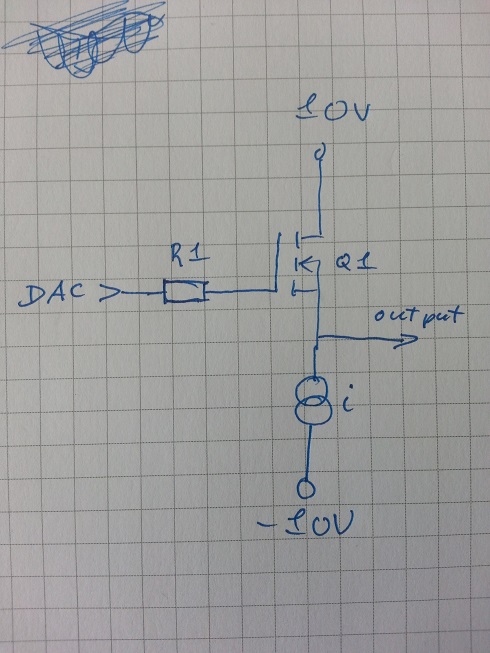
1) Find a suitable MOSFET with a low Ciss and a Vgs of 2.5 V at about 10 mA.
2) design and build a current source that results in zero volt DC at the source of the MOSFET.
🙂
The gate-source threshold voltage for the IRF610 is in the range 2 - 4 V with a drain current of 250 uA. So you might end up with a idle current below 1 mA and that is IMHO to low.
I would go for the ZVN3310A. Despite it's low maximum power dissipation.
I would go for the ZVN3310A. Despite it's low maximum power dissipation.
The gate-source threshold voltage for the IRF610 is in the range 2 - 4 V with a drain current of 250 uA. So you might end up with a idle current below 1 mA and that is IMHO to low.
I would go for the ZVN3310A. Despite it's low maximum power dissipation.
looking at ZVN3310A data sheet it seems that 2.5V bias is on the low range for Ia. another candidate more appropriate for this gate voltage?
it seems were are closer now that of the beginning of the thread 🙂
eureka ! a voltage shifter from the drain in this case ( mosfet follower)
thanls ZM 🙂
one last question can i just put a 1k resistor in place of the CCS at first time. and if i go dc coupled with my dac i just let the gate floating with no reference to ground ?
thanls ZM 🙂
one last question can i just put a 1k resistor in place of the CCS at first time. and if i go dc coupled with my dac i just let the gate floating with no reference to ground ?
Last edited:
- Status
- Not open for further replies.
- Home
- Amplifiers
- Pass Labs
- best buffer for DC coupling