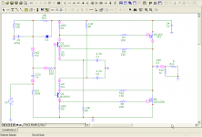
No, it doesn't make a difference. R14 is there to set the bases at 12V (half PS voltage) and to determine resistive value of Zin. R18's 220R doesn't change anything in that regard. R18 is there just to slightly isolate the bases and to provide some serial resistance in the input circuit should the input LP filter cap be needed.
Of course, since you intend to use TO3 devices (k135/j50) it would be nice to rearrange the output LatFETs connections in appropriate manner - Source and Drain of the upper LatFET can trade their places so there will be no need for a jumper and the Drain trace can be thicker and shorter. The same goes for lower LatFET's Gate and Source pins.
Of course, since you intend to use TO3 devices (k135/j50) it would be nice to rearrange the output LatFETs connections in appropriate manner - Source and Drain of the upper LatFET can trade their places so there will be no need for a jumper and the Drain trace can be thicker and shorter. The same goes for lower LatFET's Gate and Source pins.
Last edited:
I'm afraid that not understanding that one disqualifies you as a critic, but here it is:
R12/R13 create a voltage divider which central point is held stiff at 12V (half PS voltage) with C4 which filters the residual ripple from the rail and that is the voltage set through R14 to the bases of Q1/Q2 and through the feedback network to the drains of LatFETs. R14 predominantly determines the Zin of the amp (since the base currents of Q1/Q2 are very low) and D1 takes care of C4's discharge.
Build a quick prototype and be amazed how nice it works...
Before posting any further comments, I want to begin by clarifying two aspects:
- I'm not a critic nor a professor.
- I never thought to put myself in competition with anyone.
So to see if there was some truth in those of my insights, I had to simulate your circuit and then break it down into its basic skeleton to pull out any imbalances that at first glance do not seem to be there.
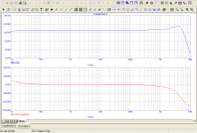
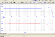
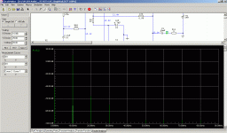
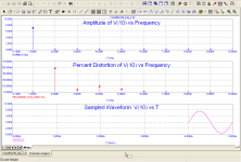
Here I attach the simulations of the original circuit completed with transient analysis, frequency response and distortion.
Attachments
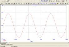
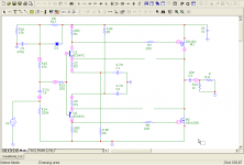
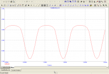
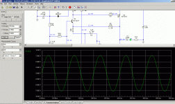
In the pictures below I removed the two resistors in the feedback loop to eliminate the effects of masking due to the reaction. I also rearranged the value of the two emitter resistors to bring the bias current of the output stage to their original values. Obviously also the value of the signal generator has been adjusted to have the same output level as the previous case.
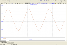
The result is very clear to me:
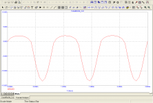
The circuit does not work in a symmetrical manner. The upper mosfet behaves as a follower and does not amplify in voltage for which the positive half-waves do not reach the amplitudes of the negative half-waves where they are amplified in voltage by the lower mosfet.
The result is very clear to me:
The circuit does not work in a symmetrical manner. The upper mosfet behaves as a follower and does not amplify in voltage for which the positive half-waves do not reach the amplitudes of the negative half-waves where they are amplified in voltage by the lower mosfet.
Attachments
Hi mos57
You seem to have Microcap simulator. How do you configure it to measure harmonics like that?
Thanks
Fab
Hi Fab, send me a PM, so i may answer your question in detail
Ok, I will !Hi Fab, send me a PM, so i may answer your question in detail
Thanks
Fab
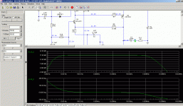
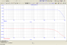
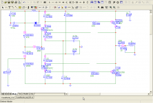
In this post I entered the circuit of Yuma modified only where strictly necessary to work with a dual power supply and below you can see the results of measurements that are substantially identical to that of the original circuit (post 22).
What do you earn?
A considerable simplification: in particular with elimination of large reactive elements or as a minimum reducing them. Another aspect is the elimination of the bias circuit of the input transistors of avoiding noise and ripple originating in power stage goes to dirty the input signal.
Attachments
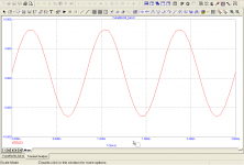
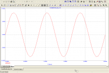
And now the real test!
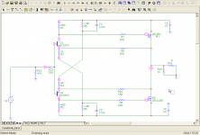
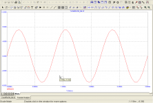
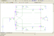
the circuit with dual power supply, but without feedback loop.
The examination shows that the output voltage of this circuit is really balanced and confirms what I have written and intuition in previous posts.
This circuit is more suitable to work natively with dual power supply than with single power supply.
Tomorrow I will present an optimized version.
Good night!
Attachments
Member
Joined 2009
Paid Member
... Said the Dorothy and went to Oz...And now the real test! ...
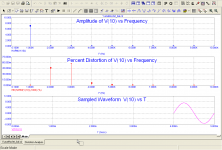
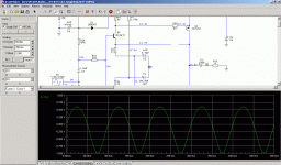
I made this amp for real and sims can be made to show anything you want so I use them only for simple calculations to save the time spent with calculator.
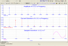
But if you want sims here you go: DC values, frequency/phase plot, transient analysis, Fourier analysis. I used highly unmatched LatFETs (see Vgs difference) to provoke high H2 and it's still 80dB below the signal...
Attachments
with such simple topologies you can have poor PSRR, is there a way to improve it ?
Yes Garreth, at expense of simplicity.
Differential input stage and CCS might be one solution.
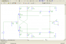
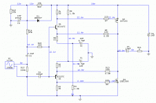
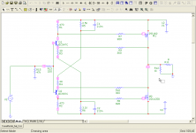
Schematic with dual power supply, revised in some small parameters to optimize its performance.
With these small changes we have obtained:
An extended and flat frequency response, an overall lower distortion.
(in particular, 3rd harmonic is decreased by almost an order of magnitude).
All this by biasing the final stage with a value less than the original circuit.
With these small changes we have obtained:
An extended and flat frequency response, an overall lower distortion.
(in particular, 3rd harmonic is decreased by almost an order of magnitude).
All this by biasing the final stage with a value less than the original circuit.
Attachments
I took some time to look into this charade and it's clear to me too: it's a fake - you used 6.8k resistors to limit the current through BJTs to about 1.5mA and since the feedback loop is absent and the BJTs' parameters are unequal, one of them stays current hungry and of course you'll get unsymmetrical signal at the output. So your thesis still lingers in the fairy land......The result is very clear to me: ...
Member
Joined 2009
Paid Member
Yes Garreth, at expense of simplicity.
Differential input stage and CCS might be one solution.
You could try a dual differential with a low impedance feedback network ?
I took some time to look into this charade and it's clear to me too: it's a fake - you used 6.8k resistors to limit the current through BJTs to about 1.5mA and since the feedback loop is absent and the BJTs' parameters are unequal, one of them stays current hungry and of course you'll get unsymmetrical signal at the output. So your thesis still lingers in the fairy land...
Yuma, I do not tell lies, I'm not trying to discredit your work, it's just my passion which brings me to investigate the audio topologies: the search for the best, as I think everyone here.
Perhaps the value of 6.8k has remained of one of the many iteration I've done on the circuit, but it does not change. As you can see, I brought that value to 3k so as to allow a current in the input transistor of about 3.7 mA, while the bias of the MOSFET greatly exceeds 1 A, but the result does not change.
See attached images.
Try doing simulations by yourself and you will be convinced, otherwise post here your result
in the absence of feedback the lower MOSFET works in the CE, while the upper MOSFET in CC. This is the reason of the imbalance.
Francesco
Attachments
Juma knows to design amps. Also, he makes them, not just simulate. If he is satisfied with sound, he publish them. For free. It's more than enough, isn't it?
+1
Do not forget, we also have the PCB layout.
I will built the one from Juma. Thanks for sharing your design Juma
")
Regards,
Eric
You could try a dual differential with a low impedance feedback network ?
Work is in progress. But why is the reason for low impedance feedback?
In this case the FB signal enter in the second base of differential pair.
....
See attached images.
Try doing simulations by yourself and you will be convinced, otherwise post here your result
in the absence of feedback the lower MOSFET works in the CE, while the upper MOSFET in CC. This is the reason of the imbalance.
I did some additional simulations (absent feedback loop) and I succeeded to get the result similar to yours (see attachment) by making LatFETs have very different gm (KP) and Vto parameters and the imbalance is clearly a product of different gain of LatFETs and not because of topological error.
So obviously, the imbalance you get is due to the erratic sim model you use for LatFETs which both work in Common Source mode.
Attachments
I did some additional simulations (absent feedback loop) and I succeeded to get the result similar to yours (see attachment) by making LatFETs have very different gm (KP) and Vto parameters and the imbalance is clearly a product of different gain of LatFETs and not because of topological error.
So obviously, the imbalance you get is due to the erratic sim model you use for LatFETs which both work in Common Source mode.
Your reasoning does not convice me for two reasons mainly.
- given that all the complementary pairs have more or less the same problem, one could not build amplifiers using pairs of devices.
- The same couple indicted, when simulated in the schematic with two batteries does not show these large discrepancies.
In the attached scheme to avoid overlap operation of the two devices, I deliberately under-biased the final stage where you can see a bit of cross-over distortion.
The appearance evident that it captures is that here the positive half-wave is amplified to the same level or even slightly greater than the lower one.
So the difference with your original circuit seems topological
Attachments
- Home
- Amplifiers
- Pass Labs
- Recommendation for 5-10W amp.