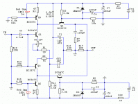
On a friend's request I did a bit different version of this preamp:
- PSU voltage is lower (+/-18V)
- Gain is lower (11db, 3.5V/V)
- Zout is lower (680R) so the buffer on the output is not mandatory
- Zin is about 21k
- max. output swing is about 13V_peak
- it's an all bjt made, no need for hard to find JFETs
- current draw is about 30mA per rail, per channel
- P1 sets the DC offset which is pretty stable if the BJT pairs are thermally coupled
The most important thing: the sound is still great...
Attachments
Last edited:
Full Monty according to Juma. Can post gerbers if anyone is interested in them.
Buzz, will ask here as you posted your pcb layout publicly
")
Do you think that transformers can cause some noise as it is close enough to the preamp part?
1. Where would you put the volume control?
2.And what's the best value?
3.Have you made a PCB layout yet?
1. At input
2. 10k
3. No. It's a 3D point-to-point construction in the recycled sat-receiver's case. That way it was easy to thermally couple the BJTs and since it's a one-time job, done in a day, I didn't want to lose the time on developing and making the PCB. I suppose I'll do it next time (if the need arises).
Anyway the result sounds so good that I decided to put it here...
one meter will be better
Seperately supplies are indeed better. I will probably remove the transformer and use the first board that has dual graetz bridge. My final version, whether SE or balanced, will use Peranders SuperReg. The decision of pre will be this or bàlanced and version of BA3.
They both sound really great - during the testing in the same system we couldn't find obvious differences, they are in domain of subtle nuances. OTOH my pre (JFET) is configured for higher gain with buffer at the output (post #66) and the BJT version for my friend (post#101) is low gain, CCS supplied current, without output buffer.
I think it would be interesting to test JFETs and BJTs in the same configuration (same gain, same PSU, same Zout). That would give more conclusive results. If you have the parts, there's a nice test you could do...
I think it would be interesting to test JFETs and BJTs in the same configuration (same gain, same PSU, same Zout). That would give more conclusive results. If you have the parts, there's a nice test you could do...
Two ways to do it:... 20db gain on BJT version...
- raise the value of R17 (it sounds better but raises the Zout too)
- lower the value of R12 (makes the pre sound murky if you go too low with it)
You can experiment with these two values to find what you like. I would make R17=2k and add a buffer at the output.
... schematic from post#66, how do you figure the gain of the folded cascode? ...
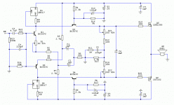
Gain of this preamp is determined as a ratio of output I/V resistor (R9=2k2) and degenerative resistance of the input stage: R6 (220R) plus parallel Source resistance of Q1 and Q2 plus series portion of P1.
Source resistance of JFET is reciprocal to its transconductance (Yfs, gm). So if 2sk170V and 2sj74V have gm of 40mS, they will have source resistance of 25R each. And if the P1 (20R) is set to its middle position we add another 10R to it and the result is that we have two times 35R in parallel connection which makes 17.5R in series with R6 which gives about 240R and your gain will be a bit less than 2k2/240R (because I neglected the emitter resistance of BJTs, which is very small anyway...)
Buzz,
reading your question again, I realized that you assume that this is a two stage design (JFETS having gain separate from BJTS) - it isn't .
This is a complementary single stage push-pull design where cascodes are just that, not the separate gain stage. You have to look at is as a whole.
True, the current through cascodes is separately setable and that's what makes the topology of this transconductance (pre)amp specific, but it's still one-stage design.
Measure with AC meter [say at 100Hz] the voltage at all nodes. Calculate Vg and dB normally, and then connect with Juma's theoretical analyses he showed above.Juma,
On the schematic from post#66, how do you figure the gain of the folded cascode? Am I correct that the FE gain is about 14 of the total 19dB?
Today I tested Indra1's proposal (post #76) and finally there's an amp without feedback loop that satisfies me completely (no objections to sound at all). It drives the 4 Ohm, 3-way sealed boxes magnificently.
I set the bias (R21, R22) at about 1.2A (LatFET's Vgs of about 2V).
Of course, the input stage PSU voltage should be higher, to use the full power potential of output FETs, but this was enough for the scope of the test. I used small LM317L as CCS (they do a surprisingly good job at 19mA - most thermally stable one active component CCS that I know of). DC offset at speaker is OK (+/-2.5mV). Zout is acceptable - measured at 100Hz and 10kHz it's about 0.25R
After all the tests I've done with it, I think I'm in love with this gain stage - a pity that I can't use it with VFETs due to their small gm which results in high Zout without feedback loop.
Once again, thank you Mr. Pass for bringing this great topology back to life.
Attachments
Questions to circuit in post #66 (Juma)
I need no more than approx. 6dB gain and my current pre has 500R output resistance and this will also be ok.
So my idea is to change R9 from 2k2 til 500R, giving lower Rout and gain. Will this be ok? Is the a price for lowering R9, and what would be the limit?
An idear would be to use 3 1k resistors for R9, one direct in circuit and the two selectable via jumpers. This would enable:
R9=1k => 12dB gain/Ro=1k
R9=1k//1k => 6dB gain/Ro=500R
R9=1k//1k//1k => 3dB gain/Ro=333R
Another issue is supply voltage. Would e.g. +/-12V ruin performance?
Today I tested Indra1's proposal (post #76) and finally there's an amp without feedback loop that satisfies me completely (no objections to sound at all). It drives the 4 Ohm, 3-way sealed boxes magnificently.
I set the bias (R21, R22) at about 1.2A (LatFET's Vgs of about 2V).
Of course, the input stage PSU voltage should be higher, to use the full power potential of output FETs, but this was enough for the scope of the test. I used small LM317L as CCS (they do a surprisingly good job at 19mA - most thermally stable one active component CCS that I know of). DC offset at speaker is OK (+/-2.5mV). Zout is acceptable - measured at 100Hz and 10kHz it's about 0.25R
After all the tests I've done with it, I think I'm in love with this gain stage - a pity that I can't use it with VFETs due to their small gm which results in high Zout without feedback loop.
Once again, thank you Mr. Pass for bringing this great topology back to life.
What sort of output power can we have with this circuit?
- Home
- Amplifiers
- Pass Labs
- LSK pre - BAF 2013