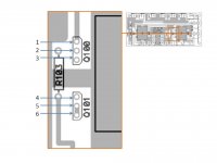
the fact that pins 5 and 6 are shorted is your clue. That means they are the gate and drain, You can then assume due to the silkscreening that pins 2 and 3 are also gate and drain.
Interestingly I believe that (at least for Q101) it will work regardless of which way around the jfet is installed")
Tony.
Interestingly I believe that (at least for Q101) it will work regardless of which way around the jfet is installed
Tony.
Shorting of pins 5 & 6 probably indicates this is a CCS to load the other tansistor.
If this is so, then 5 & 6 are gate and source, NOT gate and drain.
That then draws me to conclude that pins 1 & 4 are drains, if pin1 is connected to +ve.
That would match with a DGS pin arrangement (as 6l6 states for k170).
If this is so, then 5 & 6 are gate and source, NOT gate and drain.
That then draws me to conclude that pins 1 & 4 are drains, if pin1 is connected to +ve.
That would match with a DGS pin arrangement (as 6l6 states for k170).
Hi Andrew, from Nelson's B1 article....
http://www.enjoythemusic.com/diy/0708/first_watt_b1_preamplifier.htm
As I said as far as I am aware you can do it either way for the CCS.
Tony.
Q101 and Q201 are constant current sources formed by simply attaching the Gate pins of the JFETs to the Drain pins. They provide without loading them down or creating significant distortion.
http://www.enjoythemusic.com/diy/0708/first_watt_b1_preamplifier.htm
As I said as far as I am aware you can do it either way for the CCS.
Tony.
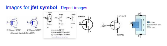
Hi Andrew, well the same misprint is in the original B1 article on passdiy I'm surprised that no one has picked it up before now!! If I google jfet symbols, some turn up with Drain above and source below, and some turn up the other way around... I guess in my prototype I have them reversed!!
Attached is the second thing that comes up in google. Note the second last image. I guess it is a good thing that they tend to be symmetrical
Tony.
I'm surprised that no one has picked it up before now!! If I google jfet symbols, some turn up with Drain above and source below, and some turn up the other way around... I guess in my prototype I have them reversed!! Attached is the second thing that comes up in google. Note the second last image. I guess it is a good thing that they tend to be symmetrical
Tony.
Attachments
Last edited:
hi Tony
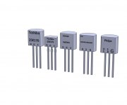
(some of them is out of stock and there are different pin orders.)
I assume that if we will stick the original Toshiba and
as long as we will keep the middle pin – as the Gate.:
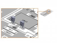
1.It can be placed according to the silk print. ( round side towards the chamfered corners ).
2.The Drain and source are symmetrical ( as you mentioned ).
3.If so ,the direction to the chamfered corners of silk print is not that important and can
be any side.
4. For the Philips and On semiconductor I will need to bend the pin in order to get them to place.
Tanks.
Ori
Hi tony
The reason for my question is to find alternative for the Jfet. (some of them is out of stock and there are different pin orders.)
I assume that if we will stick the original Toshiba and
as long as we will keep the middle pin – as the Gate.:
1.It can be placed according to the silk print. ( round side towards the chamfered corners ).
2.The Drain and source are symmetrical ( as you mentioned ).
3.If so ,the direction to the chamfered corners of silk print is not that important and can
be any side.
4. For the Philips and On semiconductor I will need to bend the pin in order to get them to place.
Tanks.
Ori
Attachments
Hi Ori, Andrew is correct WRT which is source and which is drain going off the schematic (rather than the text) of the B1 article. Most of the symbols show upper as drain and lower as source for the jfet. If you are planning on using another jfet other than the toshiba's I would definitely do them the right way as not all are symetrical.
I went back to the text before I posted to make sure I wasn't mixing things up, which turned out to confuse the issue I had some confusion originally over which pin was which (now I know why) but found people saying it didn't really matter (which when I tried it either way, it didn't seem to).
Tony.
I went back to the text before I posted to make sure I wasn't mixing things up, which turned out to confuse the issue
I had some confusion originally over which pin was which (now I know why) but found people saying it didn't really matter (which when I tried it either way, it didn't seem to). Tony.
- Status
- This old topic is closed. If you want to reopen this topic, contact a moderator using the "Report Post" button.
- Home
- Amplifiers
- Pass Labs
- Pass B1 Buffer Preamp help