Take long time but at the end I can attach the pictures. ")
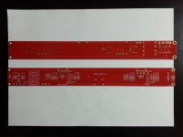
One is the F5 (red) and one is the F5T V3 (blu).
Cheers,
One is the F5 (red) and one is the F5T V3 (blu).
Cheers,
Hi to everybody on DIYAudio.
Is long time (I can say years) that I follow this forum and finally I decide to put myself on the game.
I enjoy build ampli from long time, my first ampli was a 20W in classA for car publicated by Bartolomeo Aloia. Was amazing ampli and I built 3 of them with the electronic crossover.
Coming back from the past and stopping to boring all of you...Reading almost all the threats of the PASS forum finally I decide to built a Pass ClassA. Is a hard decision because my work take me around in the word and now I am in Korea that actually is not a good place if you want to be a DIYer. Very nice people but nobody speak english and all the website (digikey and mouser included) are in korean. No way to found a part shop here in Ulsan and I get the address in Seoul (thanks DUG!) but still I don't get the chance to go there (500 km from here).
Reading the guide built of Salomon I contact him for the PCB and he suggest me to look on Jims Audio in ebay. Now I have 2 channels of F5, 2 channels of F5T v3 and 2 channels of AlepX that look very nice
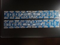
Received the V3 PCB I ordered the 5U 400 chassis from HIFI2000 that look very big and nice but reading this threat I understand that the V3 stereo in one chassis is not the best chance so I thinking come back in V2 using the PCB of V3. The picture of the board is attached. I check the PCB and look exactly as per NP schematic.
Somebody have used already this PCB? I think that can be easly used for the V2 bypassing the cascode and installing 2pr instead of 4pr.
I understand that Buzzforb have a GB for the trasformers and also can provide the Mosfet. May I ask to be part of the GB or is too late?
Any suggestion is of course most welcome!
Thanks to all of you
PS: I mention the picture of PCB... sorry, I will post when I understand how can do...
Attachments
the cap on the output is just local filtering. You may not even need it. Thermal coupling is a diyers tweak. The Pass Labs products do not have it. since moving away from the 109/369 combo, based on what i have seen in pics. It will not make you like or dislike the amp and most likely will not affect its performance in a significant way, especially considering the f5T has thermal compensation and no offset issues to speak of.
Andrew,
I am not saying that it might not make things more stable, but was is the signfigance in performance gains if you are operating with a stable amp? Do you expect decreased distortion and if so, how much? IF degenerating them and lowering overall temp, do we avoid some of these effects. Does cascoding them further diminish the effects, as it lowers overall temp. Is there any data showing the difference between coupled and non- coupled performance. I know EUVL looked into it and made a heatsink, but don't know if he had data showing the difference.
I am not saying that it might not make things more stable, but was is the signfigance in performance gains if you are operating with a stable amp? Do you expect decreased distortion and if so, how much? IF degenerating them and lowering overall temp, do we avoid some of these effects. Does cascoding them further diminish the effects, as it lowers overall temp. Is there any data showing the difference between coupled and non- coupled performance. I know EUVL looked into it and made a heatsink, but don't know if he had data showing the difference.
Would you be so kind 6L6 as to show us how you have your F5t wired now ? which way worked best with those diyaudio boards ? and how did u fix your ground loop!
Im having some issues still with the ground loops or Hum, whichever it is!
nothing beats seeing visually how it should be done! from the masters themselves ;-)
I have ground going to the gain stages first then from there to Pch and Nch boards.
atleast i got the bias problem sorted now
50 DEG, 0.31 bias
lovely!
Last edited:
I honestly don't know the part# of the thermal. It was a suggestion from another member as I found it imposible to search for on Mouser. No, you don't really need it.
5mm M3 or taller standoffs should be enough. For what it's worth, because there is so little on the small PCB that holds the Mosfets and diodes, you don't really need standoffs for those boards. It certainly doesn't hurt to have them however.
5mm M3 or taller standoffs should be enough. For what it's worth, because there is so little on the small PCB that holds the Mosfets and diodes, you don't really need standoffs for those boards. It certainly doesn't hurt to have them however.
Hi 6L6,
I'm sorry to ask this but I don't understand the different directions of your arrows on P1 and P2. My understanding was anticlockwise decreases resistance and clockwise inreases resistance. Why did you do P1 and P2 in a different way?
I remember my F5 both pots P1 and P2 where handled in the same way.
And it was my plan for my new F5T V.2 -> I turn both pots anticlockwise until I can hear a little "klick" and than start the biasing procedure.
Regarding P3: Can't I just count the whole turns from Zero to Max and then put it exactly in between? When I count correctly in total it's 62 turnings, so set it to 31 and I should have pretty much the mid of 200Ohm.
Again I'm sorry for asking such low skill questions but I better ask twice easy questions rather than blow up everything just because of a misunderstanding.
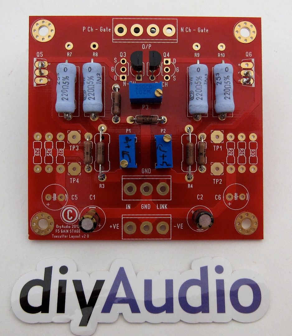
There are a couple of things that need to be done to the FE board when you are stuffing it -
1) Set P3 to it's middle value - with an ohmmeter measure from the wiper and one leg to the other leg and set the approximate middle. (about 100 ohm) Now turn the pot around, measure from the other leg and wiper to the first leg and set it to the middle value. You will find that as you flip the pot you will eventually find the equal setting. But as the pot track isn't exactly 200 ohms long, the null will not be exactly 100. (it will be very close, however.)
2) Turn the bias pots (P1, P2) all the way down. Measure that before soldering. Then make a mark on the pot to show which way increases the resistance.
The pots are mounted to match the PCB. Anticlockwise is only "down" if the PCB and pot are arranged to react that way. So "Down" will be whatever direction gives you the lowest reading across TP1-TP2 and TP3-TP4.
Yes, you can take P3 all the way to one direction and then go back halfway.
Yes, you can take P3 all the way to one direction and then go back halfway.
Ok, that means on the gain stage pcb v.2.2 before starting biasing process :
P2 has to be turned anticlockwise to Zero (between TP1-TP2) and
P1 has to be turned clockwise to zero (between TP3 - TP4)
---> CORRECT?
P2 has to be turned anticlockwise to Zero (between TP1-TP2) and
P1 has to be turned clockwise to zero (between TP3 - TP4)
---> CORRECT?
The pots are mounted to match the PCB. Anticlockwise is only "down" if the PCB and pot are arranged to react that way. So "Down" will be whatever direction gives you the lowest reading across TP1-TP2 and TP3-TP4.
Yes, you can take P3 all the way to one direction and then go back halfway.
- Home
- Amplifiers
- Pass Labs
- Building an F5 Turbo v2 (in-Progress)