PKI,
Degenerating the J74 more gets you lower second harmonic, I believe, as it has a naturally higher Yfs(transconductance). Check out Euvl's F5X build thread. He talks about matching the input jfets to null the 2k harmonic by changing the Rs used. I thought it was in the f5T article, but not shockingly, I did not remember correctly. Side note, you also have to consider the output stage as well, as it also contributes to signal gain. P3 adjust amp harmonic balance by affecting FE balace, as the output stage could only be manipulated by differing their Rs.
Degenerating the J74 more gets you lower second harmonic, I believe, as it has a naturally higher Yfs(transconductance). Check out Euvl's F5X build thread. He talks about matching the input jfets to null the 2k harmonic by changing the Rs used. I thought it was in the f5T article, but not shockingly, I did not remember correctly. Side note, you also have to consider the output stage as well, as it also contributes to signal gain. P3 adjust amp harmonic balance by affecting FE balace, as the output stage could only be manipulated by differing their Rs.
so i must admit that I was puzzled that it was the J74 that had to be degenerated to ull 2d, as this seemed counterintuitive, but then i remembered from the f6 thread that you there is more than one variable. Found this in BA3 article. It relates to what I said about considering that the amp is two stage and you are not just affecting the harmonic disatribution, but also the phase, realtive to the input signal.
Ah what a tangled web we weave. I believe PKI can testify to the very audible difference
"Potentiometer P3 is provided for those of you who have distortion analyzers or want to play with the mix of second vs third harmonic. As with the F5 amplifier, you will find that you can iteratively trim P1 through P3 for minimum distortion. I do so at approximately the 1 watt output level (2.8 V). You should start out with the setting at the mid-point. The minimum distortion point will generally be where the plus and minus halves of the amplifier balance to such a degree as to null out the second harmonic. By introducing an imbalance you can variably re-introduce the second harmonic, and depending on which way you turn the pot, you can choose the absolute phase of the second harmonic.
I knew you would like a choice."
NP
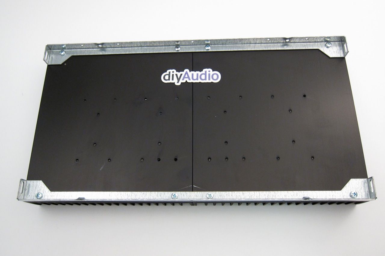
Now with the baseplate about half complete, it's time to start on the heatsinks.
This shows the upright orientation of the heatsink -- the UMS holes sit slightly low on the heatsink, to help place the transistors in the middle. Also the heatsink halves are not identical, they are actually mirror images, so when you attach the mounting brackets the holes should be even spaced across the face of the assembly.
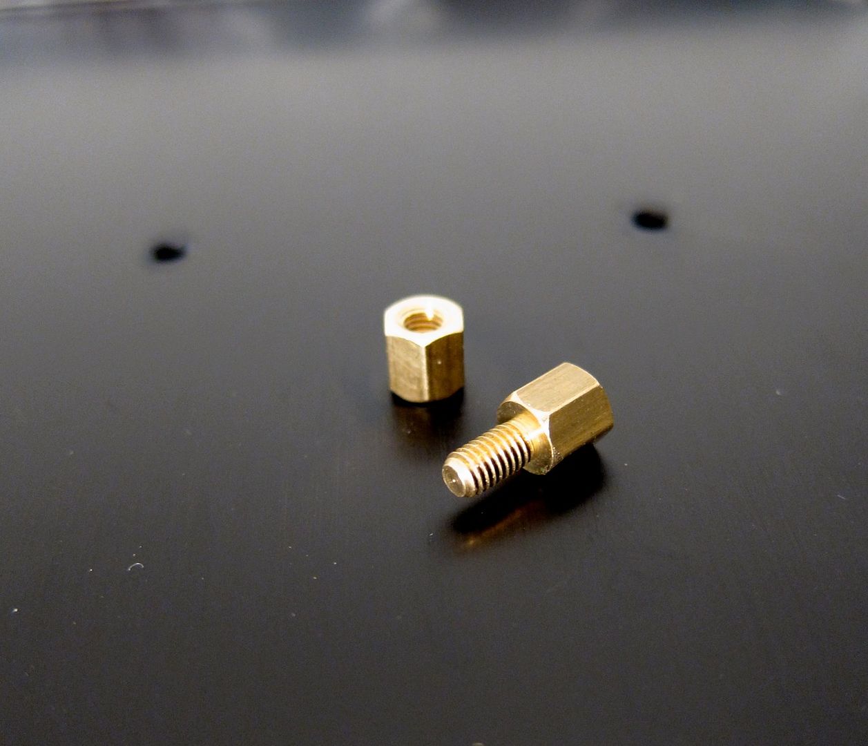
These gorgeous little brass widgets are the PCB standoffs. They screw into the heatisnk, and with 8 per side you should have this pattern --
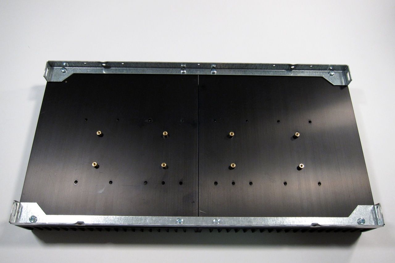
Ok, looking good, let's add the PCB and see how things line up --
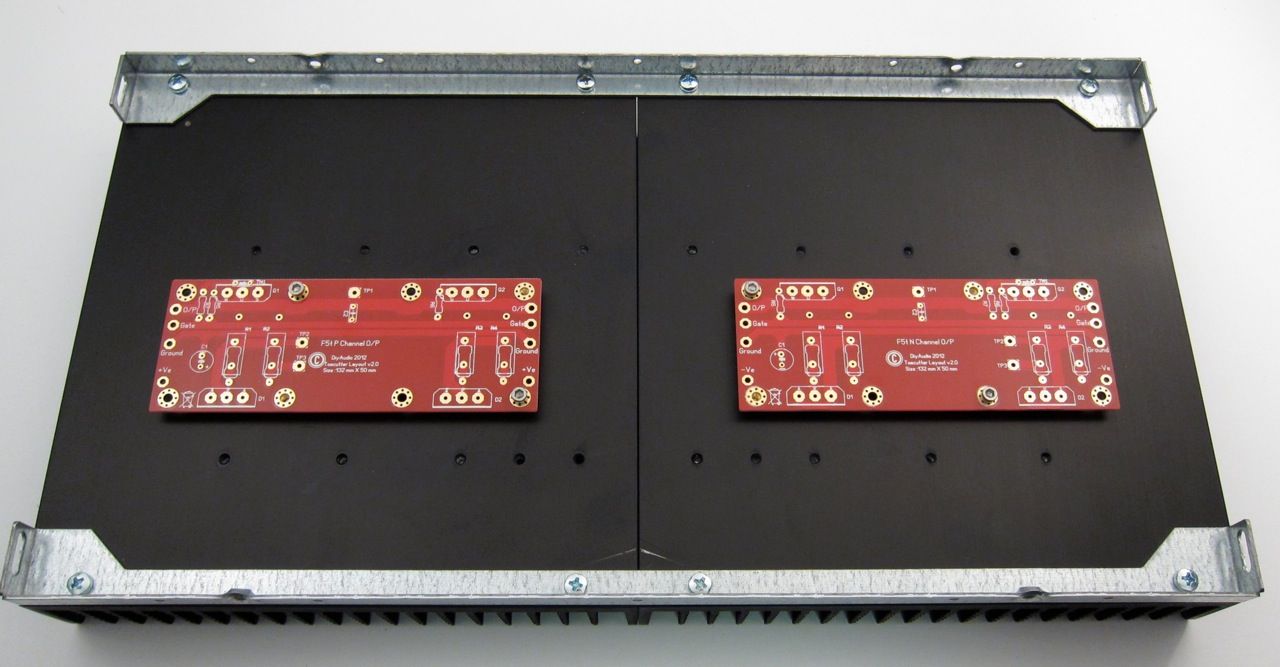
Nice! You can see that it's only held in by a couple of screws at this point, we still need to stuff the output PCBs, and mount the transistors.
I didn't get a photo of the board stuffing in-progress, but I did get it to this point before needing to fit it to the heatsink.
If you have any spare trimmed-off resistor leads (lol, of course you will...) you can make a little loop as shown and put them in the test point pads. This will facilitate the bias and test process if you have a meter with clip leads. (And honestly, if you don't you should get some.)
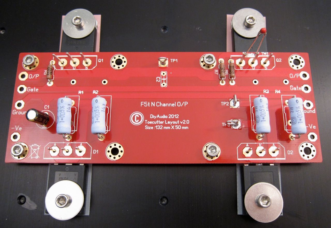
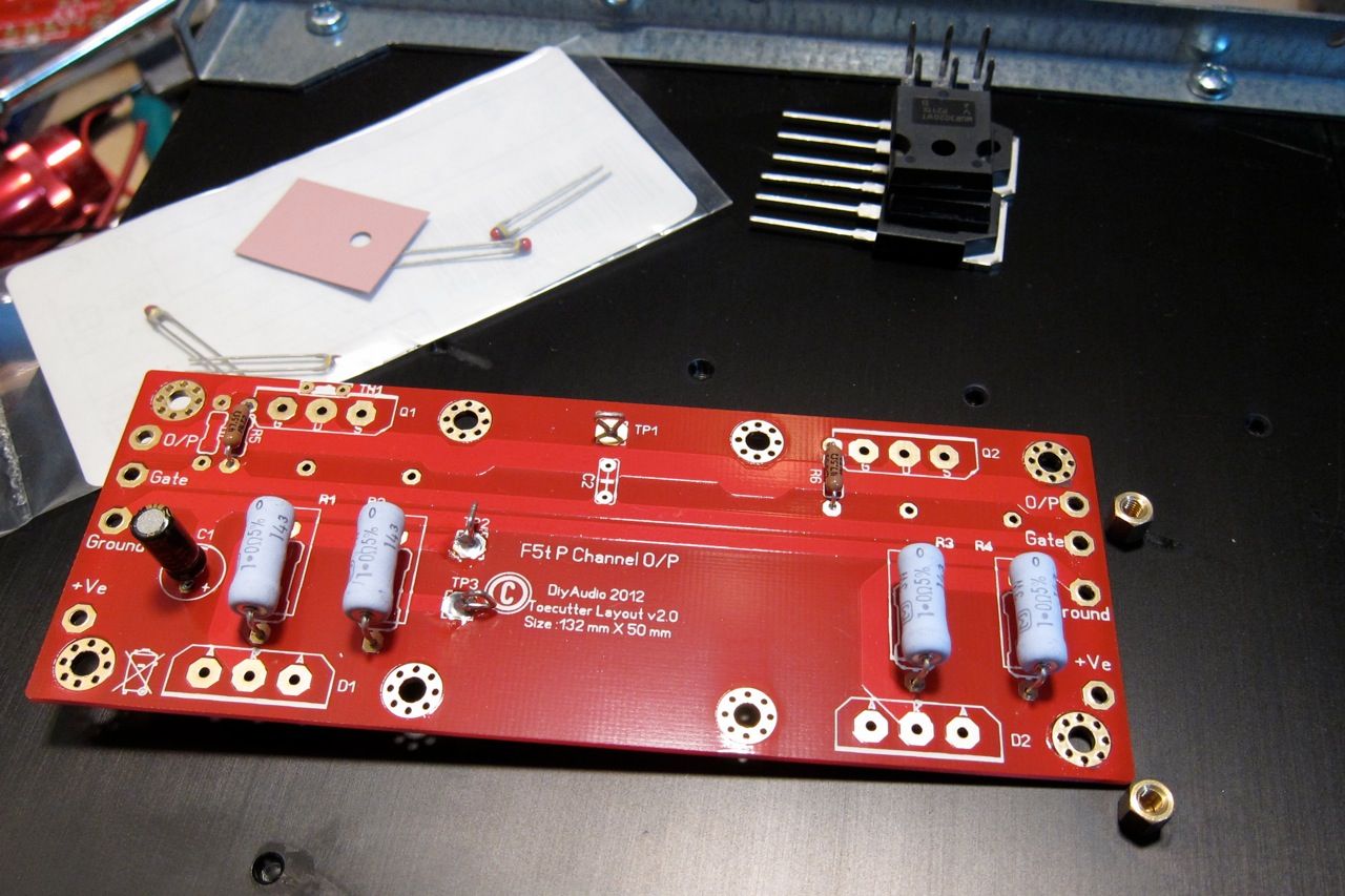
Here is a photo of the transistors (top) and diodes (bottom) mounted, with their leads bent, with silpads underneath and fender washers on top. Once everything is fit, snug, and lined up, then you can solder, trim, and also bend the thermistor.
Note - the only reason I used the grey silpads on the diodes is I didn't have enough of the pink ones to go around. Order a bunch of the pink ones and use them everywhere, diodes, bridge, transistors. The specific part number (from Mouser) will be specified in the BOM.
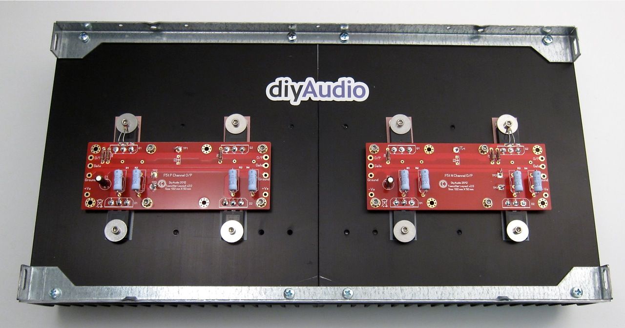
Mount and solder everything (with the N channel on the Right side, the P on the Left) and the heatsink should now look like this.
~
The Front-End board needs to be stuffed as per the version you are building… This shows a non-cascode build.
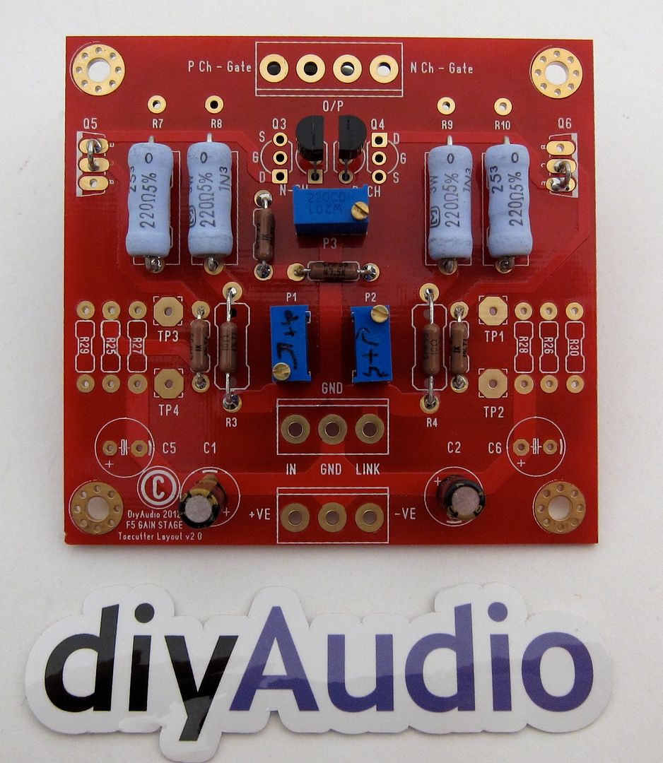
There are a couple of things that need to be done to the FE board when you are stuffing it -
1) Set P3 to it's middle value - with an ohmmeter measure from the wiper and one leg to the other leg and set the approximate middle. (about 100 ohm) Now turn the pot around, measure from the other leg and wiper to the first leg and set it to the middle value. You will find that as you flip the pot you will eventually find the equal setting. But as the pot track isn't exactly 200 ohms long, the null will not be exactly 100. (it will be very close, however.)
2) Turn the bias pots (P1, P2) all the way down. Measure that before soldering. Then make a mark on the pot to show which way increases the resistance.
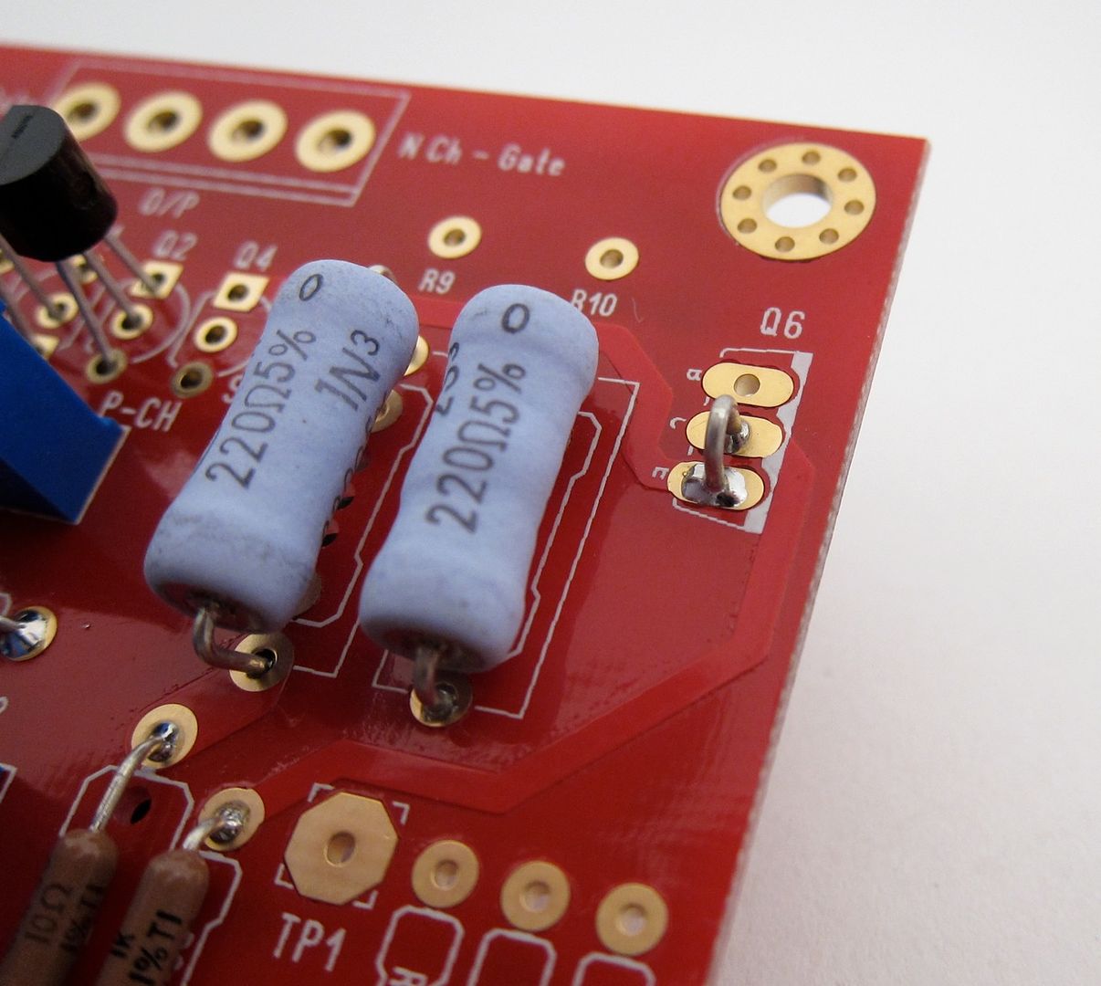
3) Make a jumper to connect C to E on Q5 and Q6. Shown below --
Yes, I know the transistors are not soldered… I put some generic TO-92 devices in the holes for the photos.
This shows the upright orientation of the heatsink -- the UMS holes sit slightly low on the heatsink, to help place the transistors in the middle. Also the heatsink halves are not identical, they are actually mirror images, so when you attach the mounting brackets the holes should be even spaced across the face of the assembly.
These gorgeous little brass widgets are the PCB standoffs. They screw into the heatisnk, and with 8 per side you should have this pattern --
Ok, looking good, let's add the PCB and see how things line up --
Nice! You can see that it's only held in by a couple of screws at this point, we still need to stuff the output PCBs, and mount the transistors.
I didn't get a photo of the board stuffing in-progress, but I did get it to this point before needing to fit it to the heatsink.
If you have any spare trimmed-off resistor leads (lol, of course you will...) you can make a little loop as shown and put them in the test point pads. This will facilitate the bias and test process if you have a meter with clip leads. (And honestly, if you don't you should get some.)
Here is a photo of the transistors (top) and diodes (bottom) mounted, with their leads bent, with silpads underneath and fender washers on top. Once everything is fit, snug, and lined up, then you can solder, trim, and also bend the thermistor.
Note - the only reason I used the grey silpads on the diodes is I didn't have enough of the pink ones to go around. Order a bunch of the pink ones and use them everywhere, diodes, bridge, transistors. The specific part number (from Mouser) will be specified in the BOM.
Mount and solder everything (with the N channel on the Right side, the P on the Left) and the heatsink should now look like this.
~
The Front-End board needs to be stuffed as per the version you are building… This shows a non-cascode build.
There are a couple of things that need to be done to the FE board when you are stuffing it -
1) Set P3 to it's middle value - with an ohmmeter measure from the wiper and one leg to the other leg and set the approximate middle. (about 100 ohm) Now turn the pot around, measure from the other leg and wiper to the first leg and set it to the middle value. You will find that as you flip the pot you will eventually find the equal setting. But as the pot track isn't exactly 200 ohms long, the null will not be exactly 100. (it will be very close, however.)
2) Turn the bias pots (P1, P2) all the way down. Measure that before soldering. Then make a mark on the pot to show which way increases the resistance.
3) Make a jumper to connect C to E on Q5 and Q6. Shown below --
Yes, I know the transistors are not soldered… I put some generic TO-92 devices in the holes for the photos.
Last edited:
The question is: can I stack transformers on a top of each other? It will help me to put them far from the boards and save me some space for nicer wiring. However, I do not want them to be coupled though the "leaking" magnetic field... and I have no idea how it is important.
I can make some estimations, but being a theorist I know how far can it be from reality ;-). Thats why I'd like to rely on engineering experience
Buzz, I did the same thing on my aleph's trims half a year ago, I used a different color, but patent is pending ;-)
I can make some estimations, but being a theorist I know how far can it be from reality ;-). Thats why I'd like to rely on engineering experience
Buzz, I did the same thing on my aleph's trims half a year ago, I used a different color, but patent is pending ;-)
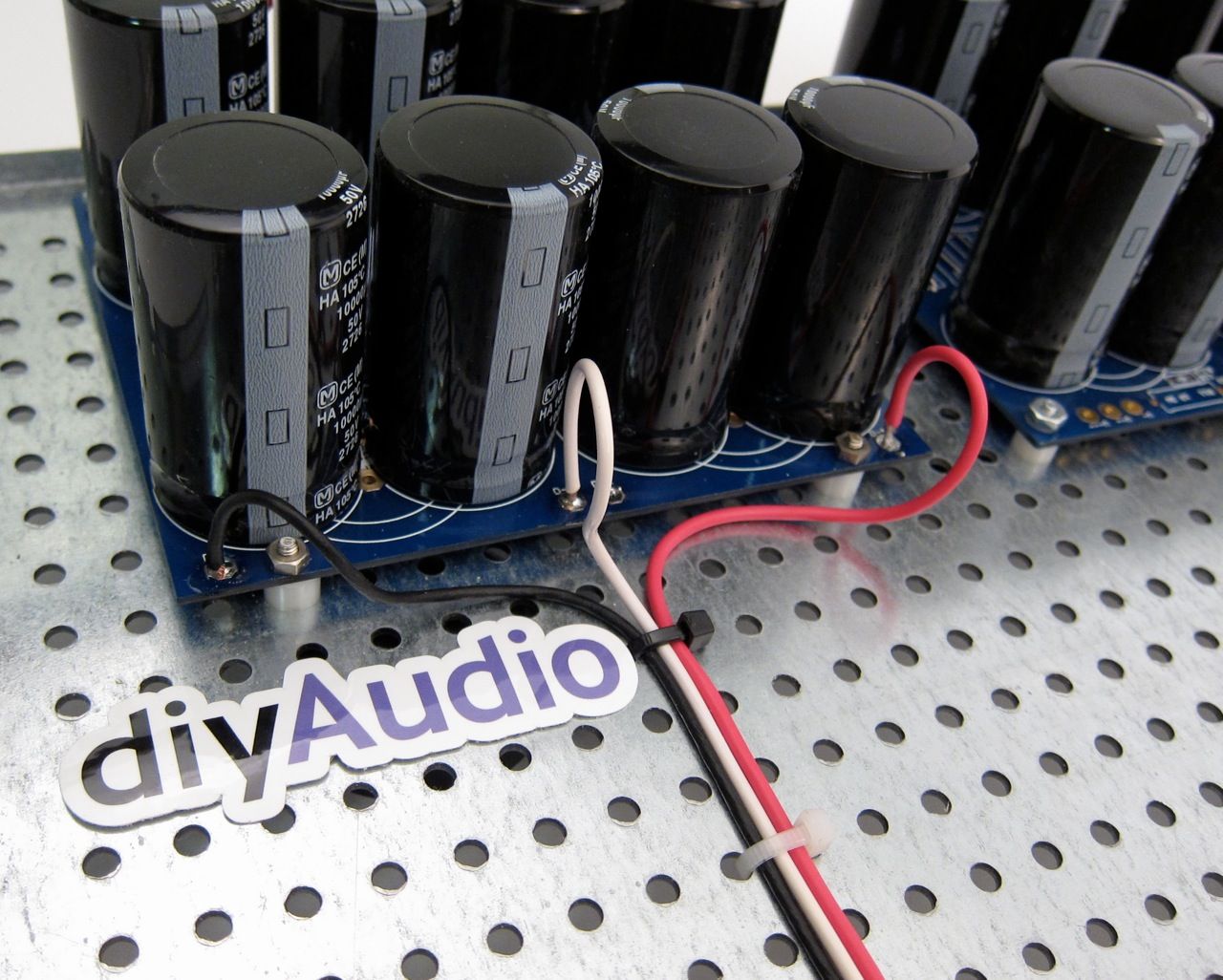
Sorry I didn't see this sooner...6L6: how did you configure the first PSU board with the filter resistors so that all 8 caps are connected BEFORE the resistors (and not 2 caps before the resistors and 2 caps after them per rail)?
I didn't.
On the first board there are 4 caps after the bridge, then the resistors, then the next 4. The next board is connected in series via some wire, where there are 8 caps. The resistor postions need to be jumpered on the 2nd board. Also on the second board is where the bleeder and LEDs are mounted.
There wasn't an easy and clean-looking way to evenly divide the 2 cap banks. That said, this could be considered a CRCRCRC filter, as the wire and jumpers have some resistance.
a) V2 or V3 monoblocks? In either case you would only need one Front-End board.
b) The V3 would need the cascode transistors in the Front-End, and their associated parts, and the pictured output boards and power supply would be for one channel. I.E., what you see so far (and the other heatsinks, which you haven't seen yet,) would be for one monoblock channel.
The rule of thumb is that a stereo V2 or a mono V3 will be in a 5U 400mm 'Big Amp Chassis'
V3 monoblocks (but since the answer is the same, I guess it does not matter?).
Darn, so I will have to buy 2 5U 'Big Amp chassis'? Time to buy some chocolates and a bunch of flowers for the spouse.
Darn, so I will have to buy 2 5U 'Big Amp chassis'? Time to buy some chocolates and a bunch of flowers for the spouse.
a) V2 or V3 monoblocks? In either case you would only need one Front-End board.
b) The V3 would need the cascode transistors in the Front-End, and their associated parts, and the pictured output boards and power supply would be for one channel. I.E., what you see so far (and the other heatsinks, which you haven't seen yet,) would be for one monoblock channel.
The rule of thumb is that a stereo V2 or a mono V3 will be in a 5U 400mm 'Big Amp Chassis'
Lol, yes, you will need basically 2 of everything you are seeing in this guide.
The (stereo) V2 PSU will be good for one V3 monoblock, the 5U 400mm chassis will hold either a stereo v2 or mono v3 etc...
I just though of something -- I bet that with just a little creativity you could make a BA-3 front-end (which is a great preamp gainstage) on the F5T Front-end boards... The circuit isn't all that different, and there are lots of places to mount things on this particular PCB. And if you are building monoblocks, you will have a pair of FE boards extra...
THIS IS EXACTLY WHY YOU NEED A LIGHT BULB MAINS LEAD --
Look at this photo:
It looks good, yes? It's not. The wire color from the rectifier is logical - Black is V-, white is GND, and red is V+. Looking at the polarity of the caps, it seems that the leads are going to the proper place... but the board isn't setup that way, and the polarity of the caps looks backwards to how it's wired.
The PCB is marked correctly. I didn't double check the markings, and got it backwards.
I tested the amp PSU with a bench-top power supply, and this this the first time it has been powered on it's own.
The only thing that saved me from letting the smoke out was the current-limiting of the light bulb mains tester.
I have been smart and lucky enough to always turn on everything during building and testing with the light bulb mains lead first to save me from my own mistakes.
I think I have seen this somewhere before on diyaudio (http://www.diyaudio.com/forums/power-supplies/164729-mains-light-bulb-tester.html), but would it be possible for you to upload a photo of where the light bulb is connected in your circuit? 100W bulb?
Last edited:
- Home
- Amplifiers
- Pass Labs
- Building an F5 Turbo v2 (in-Progress)