In what I have experienced, yes.
The first time I got it stable was with the 1000pF compensation cap ( marked C3 and C4 in the V3 schematic) and 680ohm gate resistors (R13-16 in the V2 schematic)
have you tried this amp with high idds j-fets? say 8-10mA.
For those of use without all of the insight most of you have, could you explain what C2 is doing in the circuit? I've read how Nelson states it may be needed to control ringing, and I'm looking at the schematic of V3 where C2 is shown as C3 and C4. Is it simply passing AC at a given bandwidth to the drains of the MOSFET where the given unwanted signal adds to negative feedback through the feedback resistors to the JFETs? Please excuse this simplistic explanation if it is way off base. Just trying to learn here. Thanks.
A bit more progress -- Well, actually a bunch of progress, as I have a fully-functioning stereo amplifier...
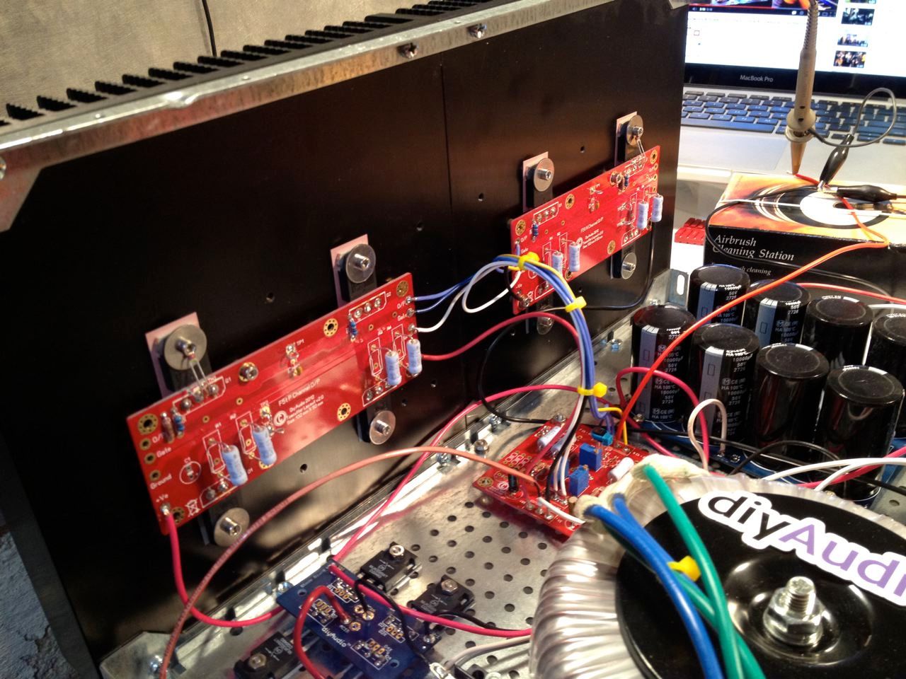
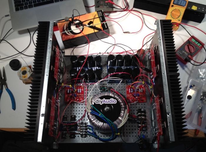
The good news - it is stable, it is working, the 5U chassis is keeping the heatsinks around 120F (49C) with .35v bias across the source resistors. There is room for more bias current.
The bad news is I currently have a ground loop problem, most likely due to the PSU wiring and general lack of wire organization. I knew I had a layout problem before I started, and wanted to utilize the DIY-friendly base as much as possible, but it's not optimal for this in it's current iteration. I have to get the bridge closer to the input caps and the FE board further from the transformer. I would like to have the wiring bundle a bit more organized, but that will happen regardless, I just plain cut some wires too long.
Concerning layout I have 2 ideas --
A) Place the FE board on the back panel. There's plenty of room in-between the RCA and Speaker jacks. That would get the driver board away from the transformer, but the wire bundle is still long.
B) Make a mount from long standoffs and some non-conductive material (Waferboard/perfboard comes to mind) and attach to the heatsink in-between and higher than the output boards. The wires would all be short. That can't be bad.
With either of those two options it will give me the space to tighten up the PSU, which is where I think the bulk of the problems are coming from. I knew the layout wasn't ideal, but vainly hoped that it would all work out. It needs a bit of work, but I'm sure it will be fine in the end.
The sound, for those of you who are curious, is completely fantastic. No surprise, really.")
The good news - it is stable, it is working, the 5U chassis is keeping the heatsinks around 120F (49C) with .35v bias across the source resistors. There is room for more bias current.
The bad news is I currently have a ground loop problem, most likely due to the PSU wiring and general lack of wire organization. I knew I had a layout problem before I started, and wanted to utilize the DIY-friendly base as much as possible, but it's not optimal for this in it's current iteration. I have to get the bridge closer to the input caps and the FE board further from the transformer. I would like to have the wiring bundle a bit more organized, but that will happen regardless, I just plain cut some wires too long.
Concerning layout I have 2 ideas --
A) Place the FE board on the back panel. There's plenty of room in-between the RCA and Speaker jacks. That would get the driver board away from the transformer, but the wire bundle is still long.
B) Make a mount from long standoffs and some non-conductive material (Waferboard/perfboard comes to mind) and attach to the heatsink in-between and higher than the output boards. The wires would all be short. That can't be bad.
With either of those two options it will give me the space to tighten up the PSU, which is where I think the bulk of the problems are coming from. I knew the layout wasn't ideal, but vainly hoped that it would all work out. It needs a bit of work, but I'm sure it will be fine in the end.
The sound, for those of you who are curious, is completely fantastic. No surprise, really.
Idea 2 is the right idea, I guess.
Shorter leads from the FE-boards to the gates of the MOSFETs is always better.
As a RF-engineer I don't like the long leads from the FE-board to the output-boards, even twisted with other (output) wires... brrrr.
I guess that is what is causing oscillation.
Remember it's a very wideband amp up to 1 MHz, it can even amplify AM signals
Last edited:
Looking good 6L6. Glad to hear of success. On the ground loop issue. Are you are sure it's ground loop or overtaxed toroid? V2 is a beast and 600VA should e a minimum. I used 400vA and had slight hum, but I think it was toroid really being pushed.
Yes ........... Are we there yet ...
Yes and no - I have made some lousy layout decisions based on the perforated base's holes... and I had the desire to use one bridge because that's how the original schematic is drawn. So cleaning up some of those issues will likely contribute to fixing the hum.
Well looks like a good job apart from those problems, and let me say Iv'e had those problems with the Zen V4 i made.
Well about to follow in your footsteps soon with a similar build if i can manage to get hold of the diyaudio PCB's
Yes ........... Are we there yet ...
Yes. I have v3 populated and ready to mount. It is on TeaBags boards.I will fire it up in next few days. I have folks chomping at the bit for their kits and this is taking up my time. V3 will go head to head with F6X this weekend.
Not sure it's an X, just sounds cool.
http://www.diyaudio.com/forums/pass-labs/233101-funny-6-a.html
My understanding is that it forms a low-pass filter for the very high frequencies, well above the audible range. I have given the amp 100K square and sine waves and they still look fine, so the corner frequency is probably quite a bit above that. It's to stop oscillation way up there.
Hopefully somebody smarter than I can give a better explanation. (Please)
Hopefully somebody smarter than I can give a better explanation. (Please)
- Home
- Amplifiers
- Pass Labs
- Building an F5 Turbo v2 (in-Progress)