Thank you Dr. Mazzola for your second article. Like the first, it clearly shows that you've put a lot of effort, thought and time into it, and is greatly appreciated. Got a couple of questions regarding the box you entitled "Amplifier abstraction made easy".
1. Schade feedback is prominently shown in the right hand schematic. Is it negative feedback? Is Schade feedback general in its application and benefit so as to include BJTs?
Got more questions pertaining to Figure 1 of the attached image. It belongs to a power BJT; maybe like that of 2N3055; aka Old Faithful. Is this BJT lazier than the laziest power switching FET; which consequently will give the most spacious and sweetest "Candy Land". If yes; please modify the 7 step procedure to suit. IGBT and SIT may sneak in this conversation. Where do they sit on the scale of relative switching laziness?
Thank you, and best regards
Attachments
Dear SemisouthFan,
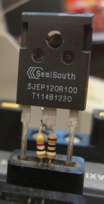
Many thanks for your wonderful contribution. It is like an anticipated birthday gift to me, as I happen to have some SJEP120R100 waiting to be used and a pair of ZCA single ended Mosfet (K1058) wonderful little amps from our mate Mark Houston, powering my third system, which is comparable to your diagram (b) from the "Amplifier abstraction made easy" box.
I use a regulated supply which can be converted to "variable regulated" supply easily from 28V to what the heatsink allows me to reduce...
Now the voltages are VDD=VPS= 24VDC, VDS= 12V. ID is something around 0,8.
I wanted to clarifye the values you propose as I intend to swap the K1058 for the SJEP120R100 and save a lot of work
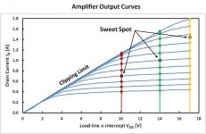
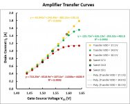
On your graphs, sometimes you plot ID againts VDD and others against VDS. If I understood well (probably not) I could reduce VDD=VPS to 17,5V and reduce R load to reach the sweet spot at ID=1,4A(?)
Did I get it or it is the other way round?
I don't need much power, I believe I am on the milliwatt range.
https://www.youtube.com/watch?v=tWuOMCUsdWU&list=UUIRNCQpvrl-EfalifsmR4KA
https://picasaweb.google.com/lh/photo/DBPGMEHS_kM2f_Pev5oCZtMTjNZETYmyPJy0liipFm0?feat=directlink
https://picasaweb.google.com/lh/photo/4QjkMa8ot0_xP7SWF06nO9MTjNZETYmyPJy0liipFm0?feat=directlink
Thank you again,
M.
Many thanks for your wonderful contribution. It is like an anticipated birthday gift to me, as I happen to have some SJEP120R100 waiting to be used and a pair of ZCA single ended Mosfet (K1058) wonderful little amps from our mate Mark Houston, powering my third system, which is comparable to your diagram (b) from the "Amplifier abstraction made easy" box.
I use a regulated supply which can be converted to "variable regulated" supply easily from 28V to what the heatsink allows me to reduce...
Now the voltages are VDD=VPS= 24VDC, VDS= 12V. ID is something around 0,8.
I wanted to clarifye the values you propose as I intend to swap the K1058 for the SJEP120R100 and save a lot of work
On your graphs, sometimes you plot ID againts VDD and others against VDS. If I understood well (probably not) I could reduce VDD=VPS to 17,5V and reduce R load to reach the sweet spot at ID=1,4A(?)
Did I get it or it is the other way round?
I don't need much power, I believe I am on the milliwatt range.
https://www.youtube.com/watch?v=tWuOMCUsdWU&list=UUIRNCQpvrl-EfalifsmR4KA
https://picasaweb.google.com/lh/photo/DBPGMEHS_kM2f_Pev5oCZtMTjNZETYmyPJy0liipFm0?feat=directlink
https://picasaweb.google.com/lh/photo/4QjkMa8ot0_xP7SWF06nO9MTjNZETYmyPJy0liipFm0?feat=directlink
Thank you again,
M.
Cool!
The R125s you sent me work great in my inductor loaded Zen amp =)
But as my PSU is a SMPS that can be trimmed from 18.65 - 23 V I guess I could test trimming the voltage up and down (compensating with current to get the same dissipation) and see if there is a magic point where the distortion is much lower than outside.
Antoinel,
Thank you for your kind comments and taking the time to look at the article. Here are my thoughts on your questions:
1. Yes, Schade feedback is negative feedback (feedback is usually understood as short for negative feedback, except when you are talking about positive feedback as in the case of oscillator circuits). The Schade feedback used in the current-source biased Pass amplifiers I'm familiar with is cleverly designed to have little "beta" or feedback factor when compared to the AC path coming from the input signal path. For example, in the F2 amplifier, R6 (100 kOhm) kills the beta for the Schade feedback of the AC modulation at the drain of the gain device. Instead, the Schade feedback is used to balance the DC bias current in the gain device (IRFP240) to be equal to the current source (IRFP9240). The same is true for the F2J except R6 is reduced to 8.2 kOhm to account for the forward bias current required of the gate-source junction of the SJEP120R100. In contrast, the input signal sees R3 at 47 Ohms. No contest. This was done to allow Schade feedback to set the DC bias of the gain device, but not to add significantly to the signal feedback beyond that supplied from source degeneracy (R7-R12).
2. Have at it with the BJT! It does look a bit chubby. My procedure works equally well for BJT's if you are careful about measuring the base-emitter voltage. In electronics text books used by electrical engineering students (and their professors), BJT's are treated as voltage controlled devices, as in fact they are. In other words, the transistor transfer curve is plotted as IC vs. VBE. You can, therefore, also plot the amplifier transfer curve as IC vs. VBE. You will see the same higher-order shape with an inflection point. On the value of BJTs in these circuits, it is my impression that expert analog circuit designers treat BJTs as the gold-standard for linearity, although the justification for this conventional wisdom, I believe, depends on the circuit. From the standpoint of load-line canceling, it does not matter what kind of transistor, all that matters is the shape of the output curves. The biggest obstacle to using a BJT is power dissipation. If you have never run up against second breakdown, you might in the kind of power-hungry Class A operation that sweet spot searchers are tempted to pursue. Second breakdown is a mortal threat to a BJT. One exposure and it is RIP! The second biggest obstacle is the forward bias current of the base-emitter junction. That leakage current in power BJTs of comparable power dissipation as the SJEP120R100 will be considerably greater than that of the JFET, which people already complain about. And it will complicate the Schade feedback design I mentioned in item (1). But hey, not every amp is a F2, so maybe one of those will work fine in your amp.
IGBTs can be used just like MOSFETs, although all of them are really optimized for switching and so they are susceptible to device killing thermal events if biased into Class A. SITs are an interesting device. I plan to cover them a bit in the third article. In general, though, my analysis has suggested to me that lower drain resistance is better for lower speaker impedances as mentioned in step 6(f) without justification (yet).
Good luck sweet spot searching!!
Thank you for your kind comments and taking the time to look at the article. Here are my thoughts on your questions:
1. Yes, Schade feedback is negative feedback (feedback is usually understood as short for negative feedback, except when you are talking about positive feedback as in the case of oscillator circuits). The Schade feedback used in the current-source biased Pass amplifiers I'm familiar with is cleverly designed to have little "beta" or feedback factor when compared to the AC path coming from the input signal path. For example, in the F2 amplifier, R6 (100 kOhm) kills the beta for the Schade feedback of the AC modulation at the drain of the gain device. Instead, the Schade feedback is used to balance the DC bias current in the gain device (IRFP240) to be equal to the current source (IRFP9240). The same is true for the F2J except R6 is reduced to 8.2 kOhm to account for the forward bias current required of the gate-source junction of the SJEP120R100. In contrast, the input signal sees R3 at 47 Ohms. No contest. This was done to allow Schade feedback to set the DC bias of the gain device, but not to add significantly to the signal feedback beyond that supplied from source degeneracy (R7-R12).
2. Have at it with the BJT! It does look a bit chubby
. My procedure works equally well for BJT's if you are careful about measuring the base-emitter voltage. In electronics text books used by electrical engineering students (and their professors), BJT's are treated as voltage controlled devices, as in fact they are. In other words, the transistor transfer curve is plotted as IC vs. VBE. You can, therefore, also plot the amplifier transfer curve as IC vs. VBE. You will see the same higher-order shape with an inflection point. On the value of BJTs in these circuits, it is my impression that expert analog circuit designers treat BJTs as the gold-standard for linearity, although the justification for this conventional wisdom, I believe, depends on the circuit. From the standpoint of load-line canceling, it does not matter what kind of transistor, all that matters is the shape of the output curves. The biggest obstacle to using a BJT is power dissipation. If you have never run up against second breakdown, you might in the kind of power-hungry Class A operation that sweet spot searchers are tempted to pursue. Second breakdown is a mortal threat to a BJT. One exposure and it is RIP! The second biggest obstacle is the forward bias current of the base-emitter junction. That leakage current in power BJTs of comparable power dissipation as the SJEP120R100 will be considerably greater than that of the JFET, which people already complain about. And it will complicate the Schade feedback design I mentioned in item (1). But hey, not every amp is a F2, so maybe one of those will work fine in your amp.IGBTs can be used just like MOSFETs, although all of them are really optimized for switching and so they are susceptible to device killing thermal events if biased into Class A. SITs are an interesting device. I plan to cover them a bit in the third article. In general, though, my analysis has suggested to me that lower drain resistance is better for lower speaker impedances as mentioned in step 6(f) without justification (yet).
Good luck sweet spot searching!!
Thank you Dr. Mazzola for your second article. Like the first, it clearly shows that you've put a lot of effort, thought and time into it, and is greatly appreciated. Got a couple of questions regarding the box you entitled "Amplifier abstraction made easy".
1. Schade feedback is prominently shown in the right hand schematic. Is it negative feedback? Is Schade feedback general in its application and benefit so as to include BJTs?
Got more questions pertaining to Figure 1 of the attached image. It belongs to a power BJT; maybe like that of 2N3055; aka Old Faithful. Is this BJT lazier than the laziest power switching FET; which consequently will give the most spacious and sweetest "Candy Land". If yes; please modify the 7 step procedure to suit. IGBT and SIT may sneak in this conversation. Where do they sit on the scale of relative switching laziness?
Thank you, and best regards
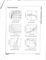
Clear images for the "How sweet it is!" box
The forum made me decrease the resolution of the pdf I posted as Part II, and I can't clearly see detail in the figures in the "How sweet it is!" box. Since this box is one of the more important parts of the article, I've attached readable versions of the images in this post.
The forum made me decrease the resolution of the pdf I posted as Part II, and I can't clearly see detail in the figures in the "How sweet it is!" box. Since this box is one of the more important parts of the article, I've attached readable versions of the images in this post.
Attachments
The forum made me decrease the resolution of the pdf I posted as Part II, and I can't clearly see detail in the figures in the "How sweet it is!" box. Since this box is one of the more important parts of the article, I've attached readable versions of the images in this post.
Great! Thanks a lot.
M.
Thank you Dr. Mazzola for your reply and clarifications in Post #365. I am glad/proud to say that you have a successful college course [for Spring 2015] entitled "What's the Buzz?; which bridges the objective transfer function of semiconductors with their subjective sound. Mr. Pass may wish to lecture this future class about his complementary point of view. Like others, I look forward to Part III.
I hope that you include in Part III:
1. Additional detail on the basis, application and especially the benefit/sonic value of Schade Feedback in semiconductor circuits; which to me is a mysterious phenomenon.
2. Simulating the performance of power SIT like that described by DIYer wrenchone in his thread entitled "L'Fake .. " in the Pass Labs Forum.
N.B. The shortcoming of BJTs that you highlighted in post #365 maybe alleviated by using LM395 K/T as a well-behaved BJT model; which was called in 1976 [or earlier by National] an "Ultra Reliable Power Transistor".
Best regards.
Hello Zen Mod. Thank you for the pdf on your blog site regarding Schade.
Best regards.
My continuing study of "What's the Buzz? Part II" led me to propose this hypothesis regarding the superb performance of THRESHOLD power amps. Their NPN and PNP transistors of the output stage which operate using the famous "STASIS" mode, operate at their Sweet Spots in Candy Land; like that described by Dr. Mazzola.
Thanks for the great ideas. I've been scoping the article in my mind. As Bob Seger's song Against the Wind goes, "what to leave in, what to leave out..."
I looked up the part you mentioned. Here's a concise description from a datasheet:
"The LM195/LM395 are fast, monolithic power integrated circuits with complete overload protection. These devices, which act as high gain power transistors, have included on the chip, current limiting, power limiting, and thermal overload protection making them virtually impossible to destroy from any type of overload."
Interesting trick and I agree it could fix both the thermal stability and the base current issue. But, without any experience at all with such a gain device (notice I don't call it a transistor), I would express caution about all that protective stuff. Could it introduce unexpected features during audio reproduction? What sort of unexpected features? Well, the overload monitoring circuitry works by influencing the transfer characteristics. In other words, I suspect the protective circuitry could create distortion in the signal being amplified. Looking at the output curves in the datasheet you can see the power limiting explicitly in the output curves. That is something to be wary about. Maybe you can give one a spin and let us know?
But the little application circuits shown in the datasheet are sooo 1976. What a great time to be a teenage DIY circuit builder! Popular Electronics, Forrest M. Mims III, Radio Shacks with stuff worth buying, beer, girls
Thank you Dr. Mazzola for your reply and clarifications in Post #365. I am glad/proud to say that you have a successful college course [for Spring 2015] entitled "What's the Buzz?; which bridges the objective transfer function of semiconductors with their subjective sound. Mr. Pass may wish to lecture this future class about his complementary point of view. Like others, I look forward to Part III.
I hope that you include in Part III:
1. Additional detail on the basis, application and especially the benefit/sonic value of Schade Feedback in semiconductor circuits; which to me is a mysterious phenomenon.
2. Simulating the performance of power SIT like that described by DIYer wrenchone in his thread entitled "L'Fake .. " in the Pass Labs Forum.
N.B. The shortcoming of BJTs that you highlighted in post #365 maybe alleviated by using LM395 K/T as a well-behaved BJT model; which was called in 1976 [or earlier by National] an "Ultra Reliable Power Transistor".
Best regards.
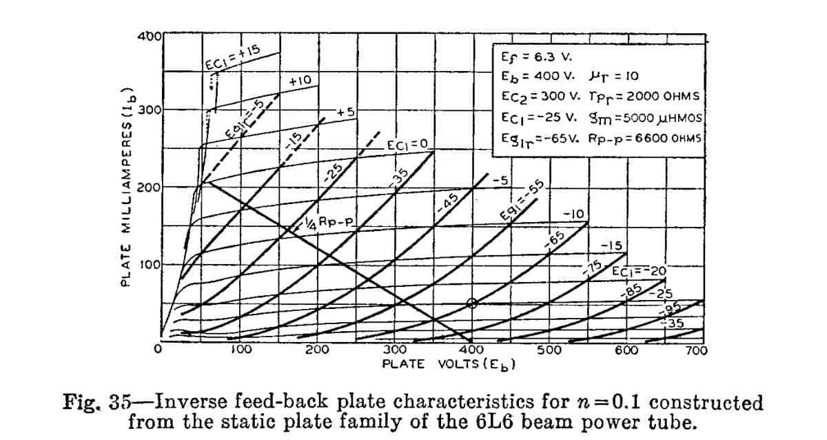
100% Schade feedback applied to a SJEP120R100 JFET on a curve tracer with an eight ohm load line superimposed. Other than the curves are upside down due to the need to trick the curve tracer, they look similar to those in O.H. Schade's original article, especially to what can be seen in Fig. 34. Definitely going to talk about this in Part III...
Attachments
. Maybe you can give one a spin and let us know?
What a great time to be a teenage DIY circuit builder! Popular Electronics, Forrest M. Mims III, Radio Shacks with stuff worth buying, beer, girls
Thank you for your comments. I hope to practice your 7 step procedure on LM395T which I have; so as to extend, and generalize the scope of this application.
During the period of 1975-1979, I was at the Champaign/Urbana campus of the University of Illinois; which was the birthplace of the Parachuting Streakers. I remember on a bright sunny day a chance encounter with possibly Mr. Pass in its auditorium for concerts; demo'ing with other competitors powerful amps driving loudspeakers with low frequencies which caused me to literally run away from their intense sound pressure. This concert auditorium hosted The Carpenters, Tom Jones and Elvis [his final performance] in addition to others which I attended. Those were the days.
Best regards.
Ha ha. We probably both listen to the 70's on 7.
Thank you for your comments. I hope to practice your 7 step procedure on LM395T which I have; so as to extend, and generalize the scope of this application.
During the period of 1975-1979, I was at the Champaign/Urbana campus of the University of Illinois; which was the birthplace of the Parachuting Streakers. I remember on a bright sunny day a chance encounter with possibly Mr. Pass in its auditorium for concerts; demo'ing with other competitors powerful amps driving loudspeakers with low frequencies which caused me to literally run away from their intense sound pressure. This concert auditorium hosted The Carpenters, Tom Jones and Elvis [his final performance] in addition to others which I attended. Those were the days.
Best regards.
Antoinel,1. Additional detail on the basis, application and especially the benefit/sonic value of Schade Feedback in semiconductor circuits; which to me is a mysterious phenomenon.
In today's terms, Schade feedback is called "Parallel Voltage Feedback" (PVF), and is not uncommon. Check out Nelson's Zen amp for a clear example of how it is used with semiconductor amplifiers.
The application of PVF reduces distortion caused by gain changes that result from changes in the load being driven. However, my simulation tests indicate that the difference in distortion between a MOSFET with and without PVF is negligible when the device is driving no load, other than RD.
The distortion-reducing (actually output resistance reducing) mechanism of PVF is quite simple;
1) The SS device output current becomes partially dependent on the output voltage due to the application of PVF.
2) Vin and PVF are average-summed at the input of the device which lowers the device's mu and gm.
3) If Vout is reduced by loading and not by a change in Vin, then this results in a proportionate increase in Vin (due to PVF), and the correct level of Vout is re-established, essentially mimicking a device with lower inherent Ro.
- Status
- This old topic is closed. If you want to reopen this topic, contact a moderator using the "Report Post" button.
- Home
- Amplifiers
- Pass Labs
- SemiSouth boiler room