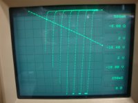
Well buzz, where did that come from? Under what other conditions? It's blurry and there is no legend so I'm gussing what most of it is. Are those Vgs trend lines? Are they -4.8V to -6V w.1V intervals ? I've seen this before I think and even played with the load line possibilties. I think I had a problem similar to you. I have other projects to finsh so I put it away for awhile...
Sure, you bet. I have an older HP and I can do DC(offset) or AC.My Toellner 7711 function generator has a DC offset function it's perhaps an useful feature in this case, isn't it?
Well, I put a little thought into it. I'm thinkin I can use the circuit attached below? Comments are welcome:
My Function Generator can produce a single + Pulse, I'm thinkin maybe 1ms long, so as not to get to much device heating. I will be going for the 25C data since anything else is a little difficult to do right now. Typically we do these measurements within 100-200uS. We'll see what the measurements look like? I can also vary the pulse amplitude in relatively small steps.
The 100 ohm should'nt induce much of any error but, save me from oscilating to death. One of those accidents I was thinkin of.
The .05 ohm Drain R is "current shunt" to measure the Ids. It's big enough to measure voltage accurately but, not big enough to eat up my Drain voltage when current is flowing. It's also big enough physically to not induce to much Tc variation from heating.
I will use a storage scope triggered on the Func Gen pulse to capture these 2 voltages. In the past I remember having to use some diodes in the set-up to avoid the scope input saturation due to the range it needs to be on but, I don't think that's an issue here. That's probably the Rdson test I'm thinkin of.
Does anyone see any issues? Have any suggestions?
The parts are pretty rugged drain to source, but at elevated Vds, I'd shoot to make the measurement in much less than 1 ms to avoid self heating. But you're already on top of that.
It's gate reverse bias that is the SemiSouth JFET's Achilles heal. Don't stress the reverse blocking of the gate-source diode unless you're prepared for the consequences.
Your concern that oscillation may produce a bad day is well founded, but your provision for 100 Ohms should be more than enough to kill the nasty oscillations before they multiply, as long as you keep the interconnections relatively tight to avoid too much gate- and drain-loop inductance.
My research team is actively working on the problem of self-oscillation with power switching circuits using SiC transistors. Our lab has dead bodies surrounding the test bed that led to our most recent paper in IEEE Transactions on Power Electronics Letters (IEEE Xplore - Stability Considerations for Silicon Carbide Field Effect Transistors). The paper is so recent it is still available only in the preview volume "99."
Ah, I forget to mention, I was carried out those measurements with an constant 9V voltage source and a 2.7 kOhm resistor.
I got exactly the same results, with all of my four SJEP120R100A.
Oh, one was lost by failure and two went to a friend for an F2J....
I still listen to those two on the left side.
and not forgotten, I got two wonderful LT1014 on a copper block from you and the pleasure hearing the F3s voice....
Do you have a picture or drawing of the "cooling" copper block ???
Or was it @Gyuri that was the creator ??
Superb
Who need SiC JFETs when the LU1014D can dissipate enough heat with your copper blocks
Last edited:
O.K. Gotta get my - and +'s in order... You are refering to never going Neg G-S? As in, make sure my Gate pulse is GND to 1.5V to GND rather than an AC signal? In my test circuit, if my Func Gen goes to -2.5V, I'll begin collecting dead soldiers... Ohh:...It's gate reverse bias that is the SemiSouth JFET's Achilles heal. Don't stress the reverse blocking of the gate-source diode unless you're prepared for the consequences...
I think we usually say "Dead Soldiers"? But today, just about anybody can claim anything is insulting or politically incorrect etc... "Dead Bugs" are other things. Probably born from the 3 legs good 8 legs bad philosophy....Our lab has dead bodies surrounding the test bed that led to our most recent paper...
I have to pay $31 to find out how to not burn one? I could not pay $31 and burn one anyway but, it cost about that when I got it. Some were $50!
And all of my devices should be pairs
Thanks

Mounting of the LU1014D device to copper spreader blocks is easy if you are skilled with SMT. You need a preheat stage, Low Temp Solder (liqiudous @140C or so), and an air pensil. Not a big deal but, DIYers have been slow to move on to SMT for various reasons. If you know what your doing, a peice of aluminium in the oven and a hair dryer can be used but the low temp solder is important.Superb

Well buzz, where did that come from? Under what other conditions? It's blurry and there is no legend so I'm gussing what most of it is. Are those Vgs trend lines? Are they -4.8V to -6V w.1V intervals ? I've seen this before I think and even played with the load line possibilties. I think I had a problem similar to you. I have other projects to finsh so I put it away for awhile...
The two images are interesting. "R085" shows the sub- to near-threshold characteristics of the depletion-mode channel design. This gives reason behind the notion that a SemiSouth depletion mode JFET can play the role of a tube and thus benefit from the higher voltage rating of the device. My business partner is an accomplished blues guitar artist and is well acquainted with the musicians love of the tube amplifier. We've been talking about the possibilities. SemiSouth put out a 650 V JFET before the end...
The "depletion jfet" image is interesting too, but if it is from the same R085, don't get too excited. This is what a common-drain (source follower) amplifier imposes on the transistor terminal characteristics. If it came from an R085, the polarity is wrong as this can't happen for positive Vds and positive Id unless Vgd is being stepped. The legend seems to show Vgs is being stepped from a negative bias. Maybe there was just a mix up in connections? Otherwise, if from the same device the two images are mutually exclusive.
Attached is an image taken of the screen of a Tektronix 370B curve tracer measuring one of my R085s with correct polarity when stepping Vgs. (Vds is on the horizontal axis at 2 V per division and is negative, Id is on the vertical axis at 0.5 A per division and also negative, Vgs is stepped in 2 V increments starting from -18 V.) I added an eight Ohm load line using the cursor function of the 370B. You can see the potential for linearity, but this is to be expected from 100% source degeneracy. The negative feedback "straightens" out the non-linearity of the transistor by using the full gain of the device.
The image represents the JFET in reverse conduction, a property of the device under intense study by my research team right now (got no choice, I have to present this research at the PCIM-Europe conference in Nuremberg in May). One caution operating this way in forward conduction by stepping Vgd: You could accidentally overstress the reverse bias on the gate-source diode of the JFET and that is a good way to create a dead JFET.
I was saving this aspect of operation for a later article, but I'll add a short section in the next one to tip the hat to the "discovery" by Buzz.
Attachments
O.K. Gotta get my - and +'s in order... You are refering to never going Neg G-S? As in, make sure my Gate pulse is GND to 1.5V to GND rather than an AC signal? In my test circuit, if my Func Gen goes to -2.5V, I'll begin collecting dead soldiers... Ohh:
I think we usually say "Dead Soldiers"? But today, just about anybody can claim anything is insulting or politically incorrect etc... "Dead Bugs" are other things. Probably born from the 3 legs good 8 legs bad philosophy.
I have to pay $31 to find out how to not burn one? I could not pay $31 and burn one anyway but, it cost about that when I got it. Some were $50!
And all of my devices should be pairs
Thanks
Yes, negative on the gate with respect to the source. But you don't have to over do it, a couple of volts negative should not be a worry unless the gate is already too leaky. (Hint, check the forward characteristics of your enhancement mode device before throwing it away because of a "shorted" gate. I have a whole sleeve full of parts that show good output curves but measure excessive gate leakage in reverse bias. For Class A amps, the "EP" parts will be biased with only positive voltage anyway. "DP" parts? Obviously, another matter.) Just be careful if the gate swings negative. The "A" models are rated at Vgs = -10 V for a reason.
for proper graphical presentation we need something as 5-6A max on ordinate and 30-35V on abscisa
only that way one can sketch proper load line , taking in account usual Iq (range) point and U/Rload point on ordinate
btw. those LU's on copper are , without doubt , Metalkidoe's work
only that way one can sketch proper load line , taking in account usual Iq (range) point and U/Rload point on ordinate
btw. those LU's on copper are , without doubt , Metalkidoe's work
I'ld like to quickly comment on this:My business partner is an accomplished blues guitar artist and is well acquainted with the musicians love of the tube amplifier. We've been talking about the possibilities. SemiSouth put out a 650 V JFET before the end...
Most musicians weather it be harp, solid/hollow body elctric Guitar, or several others, are not interested in linear distortionless amplification!
The acoustic guitar produces harmonics from the almost triangle wave of the strings due to the body shape, the wood, and construction etc. The electric only guitars/instruments depend on the harmonics created by their amp. For instance, some amps have a knob on them called overdrive. What do you think that is? As I said before about tube amplification, The soft clipping is a much "Nicer sound". Tube guitar preamps purposly over drive (to clipping) the signal and at various places in the circuit there are filters and other raz-ma-taz that gives them their signature sound. It is'nt a what goes in comes out transfer curve. I eluded to odd order distortion previously. If you have an amp with a gain(overdrive?) you can crank up to 1000, but it would be clipping at a gain of 10, your guitar will sound like Jimi Hendrix! No Sh$%^t! A square wave is essentially a fundamental sine wave, with a 3rd harmonic of 1/3 the level of the fundamental, and a 5th harmonic of 1/3rd the 3rd, and a 7th(John Curl's favorite) of 1/3rd the 5th, etc., etc, etc, A pure square wave is 33.333% THD! Pretty close to what Jimi used
It's not that their on another planet, but, it's a different goal altogether and Semiocunductors have not been able to satisfy half the guitarists out there for years!
Last edited:
for proper graphical presentation we need something as 5-6A max on ordinate and 30-35V on abscisa
only that way one can sketch proper load line , taking in account usual Iq (range) point and U/Rload point on ordinate
btw. those LU's on copper are , without doubt , Metalkidoe's work
http://www.diyaudio.com/forums/pass-labs/84605-mounting-lu1014d.html
So I tried it.
I'm not sure but, it's time to man up. I honestly thought that graph was BS for some reason but,(it looks to good!). I didn't feel like goin there with buzz or any fellow members. I think I tried to correlate the data sheet with that data and they don't match in the middle somewhere? As I said, I need a curve tracer or gumption to sit down and do it at home myself one data point at a time. We have a broken 4145 at work. I've got exp with that but, I can't fix it, our cal contracter and the Mfg want to much $$$ and I guess the designer guy's don't need it that bad?The "depletion jfet" image is interesting too, but if it is from the same R085, don't get too excited. This is what a common-drain (source follower) amplifier imposes on the transistor terminal characteristics. If it came from an R085, the polarity is wrong as this can't happen for positive Vds and positive Id unless Vgd is being stepped. The legend seems to show Vgs is being stepped from a negative bias. Maybe there was just a mix up in connections? Otherwise, if from the same device the two images are mutually exclusive...
Maybe it's the Absolut Citron Martini's? Got the driveway cleared but, their sayin it's a $500 fine to be on the road still. I don't know? this is a great thread so far, It's worth being snowed in and excersising my brain a little
And (assuming you're talking about the "depletion jfet" graph) it is too good. Any transistor with decent gain will act like that when measured that way (BJT, MOSFET, JFET, whatever). If you speak of the sub-threshold SIT like characteristics in "R085", assume they are not BS and get your curve tracer fixed.I'm not sure but, it's time to man up. I honestly thought that graph was BS for some reason but,(it looks to good!).
Maybe it's the Absolut Citron Martini's? Got the driveway cleared but, their sayin it's a $500 fine to be on the road still. I don't know? this is a great thread so far, It's worth being snowed in and excersising my brain a little
I'm in the sunny south. Martini time is right around the corner.
Sorry guy's still wading thru this post: What do you mean reverse cunduction? -Ids?The image represents the JFET in reverse conduction, a property of the device under intense study by my research team right now (got no choice, I have to present this research at the PCIM-Europe conference in Nuremberg in May). One caution operating this way in forward conduction by stepping Vgd: You could accidentally overstress the reverse bias on the gate-source diode of the JFET and that is a good way to create a dead JFET.
Seems to me I've seen an N JFET cunducting like a 2sk170 data sheet?
Your, replying to a dog. A smart dog but hey, how many dogs can read and understand most of this transistor theory? let alone type? Spelling well
- Status
- This old topic is closed. If you want to reopen this topic, contact a moderator using the "Report Post" button.
- Home
- Amplifiers
- Pass Labs
- SemiSouth boiler room