I would expect them to be very very close, especially if they are at the same temperature as previous measurements.Will jfet IDSS measure differently after burn-in, I wonder?
if you really burn them
I'd burn them in a little at a time.
A stepped/switchable resistor could be substituted.
A pot would end up with an unknown value (and unknown current) after you have played with it.
12V should be OK with all 10Vds Idss test devices.
Some devices test Idss at a lower voltage. You may have to use a lower supply for these.
You can check you circuit with higher Vds devices and see what range of voltage is applied across the Drain Source as gm and Idss is varied.
A stepped/switchable resistor could be substituted.
A pot would end up with an unknown value (and unknown current) after you have played with it.
Thank you AndrewT, you're right about ending with an unknown value! I suppose I can build a stepped resistor using a multi turn rotary switch? I have only a 4 turn switch, which I suppose won't quite cover the test range? I should have a 12 turn switch somewhere! I thought I could measure the resistance after every test, but too tedious I agree.
I could also make a 9v battery connection for devices which need lower Vds.
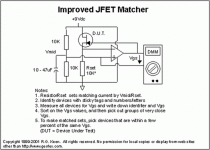
I would be very careful with this circuit because if you don't know the Idss of the DUT up front, the opamp will easily force it into positive bias.
So you need to watch Vgs very closely and slowly increase the test current.
It is useful if you want to pick JFETs at a bias known to be below its Idss.
Not useful for curve tracing unless you know exactly what you are doing.
Patrick
So you need to watch Vgs very closely and slowly increase the test current.
It is useful if you want to pick JFETs at a bias known to be below its Idss.
Not useful for curve tracing unless you know exactly what you are doing.
Patrick
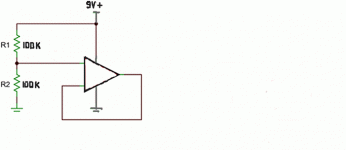
Having ordered a few T071s and resolved to a long wait, I then realized that I do have plenty of T072s on hand. So thought i'd use one of these instead! But I need to terminate one of these inputs. It's been a very long time since I did this hence hope the diagram below which I found elsewhere to which I've added the resistor values are correct.
Attachments
Last edited:
Does VGSoff of, let's say, 0.7 V actually means that's it's the maximum swing I can input to the JFET without clipping? Then how do I interface a much higher than 0.7 V pk-pk line level to it?
In a word, FEEDBACK
 either local or global.
If you are using a "Common Source" configuration with a fully bypassed Source (no local feedback), that would be correct that 0.7V pk-pk is all the signal you could handle. Some people will argue that the device can handle slightly higher, perhaps 1.1 to 1.2V pk-pk because the Gate diode doesn't start to turn on until about 0.5V. At that point THD of the output will be something in the 10% or higher range. Not very practical for audio. If the Source has degeneration, you can handle a bigger signal. A "Common Drain" configuration (~99% local feedback) can handle a signal as big as the Gate breakdown Voltage. Some circuits can handle even higher input Voltages with active power supplies.
Much like curve tracing to match fets that we know have already been characterized by the manufacturer using guess what? -a curve tracer, I find testing for Vp a waste of time and effort -we're not going to operate it at Ids=0 anyway. A curve trace might be needed if fets are suspected/found to be fakes and the seller insists they're genuine and balks to give a refund.
Find out your DC operating voltage (Vds) and your bias current (Ids) and match...heatsink it if needed and monitor temp if you can as a bonus.
Hello All,
This is a sticky thread, a place people go for reference.
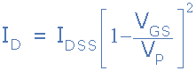
The approach Blues is taking here misses the target a bit. I agree that we are not going to use the JFET at Vp. Sometimes we do use the JFET at Idss. Knowing Vp and Idss allows us to do some calculations for the points in between on the transfer curve.
Knowing the pinchoff voltage and Idss gives us the toe and head of the transfer curve. The transfer curve provides a lot of information. gm for example.
Go to any JFET text, the first formula they give you will calculate any Id. Knowing Vp and Idss we can calculate Id for any Gate voltage. Using that selected gate voltage we can calculate the needed source resistor value.
The bit about the Vp being on the datasheet is only partially correct. The datasheet will give a range of values; any batch of JFETs can fall anywhere between the extremes of that range. Not much help.
EDIT: Without a curve tracer you can measure Id with a couple of different source resistors and using the formula you can calculate Vp.
Thanks DT
Attachments
Last edited:
Hello All,
This is a sticky thread, a place people go for reference.
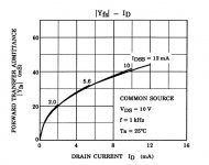
DT - A suggestion that I have made before, data is better presented as in this datasheet graph which makes it clear that for a given type of FET the Yfs (gm) is almost the same at the same Id.
As for matching most test circuits get a rather poor measure of Vp because the FET is in subthreshold operation at very low currents. The best results I have obtained were by measuring Vgs and Id at several currents staying away from subthreshold and high currents (where parasitic resistances and high current effects show up) and least squares fitting them to the ideal FET equation to get Vp and Idss. It should be noted that Vp and Idss are not independent but tend to have a constant ratio relationship (Vp/sqrt(Idss) ~ constant). In practice this is only a sort of 10% thing but it narrows the variance a lot, the curve fit narrows it a lot more. I was able to sort for complementary k170/j74 followers using the same Rsource for each device and get consistently <1-2mV offset. Letting the parts settle after touching them is critical.
You can manipulate the JFET equation to solve for the Id vs Rsource to sort FET's for complementary followers.
Excel has a solver that should work.
Attachments
Last edited:
For the same part number, Ids is all you need to measure. If this gives you too much off-set then you need a servo or a source trim-pot, not better matched parts. And gain should depend on resistors, not active part characteristics. You may enjoy fiddling with you baby, but professionals need a design that works every time with a wide range of parts.
Anyone up for the Excel curve fitting challenge?
Hello,
I believe that I have my arms around this.
From the simple practical point of view, sort the JFET’s by Id into groups centering around 1 mA steps. Then add and adjust a source resistor to dial in the desired Id for your particular application. Pretty cool. A bonus benefit to the added source resistor is reduced distortion due to modulating voltage drop across the source resistor providing feedback at the Gate.
From a more academic point of view every EE professor around the world lectures about the Shotkey JFET formula. See the formula in my post above. What the professor saves for later lectures are all the little subtleties that the Shotkey JFET model does not include. Thank you Scott for the pointers about sub-threshold low current measurements and “high” current measurements.
If you carefully and precisely measure the real world PinchOff Voltage and Idss of your favorite JFET (That is the toe and head of the transfer curve) with the idea of plugging those values into the Shotkey JFET formula your measured data points between the Vp and Idss may not fit the model very well. This may be a bit of a challenge.
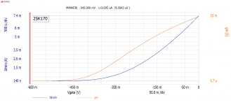
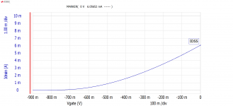
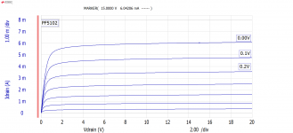
Attached are a couple sets of plots and the data set for the transfer curve. (This is for a PF5102 JFET, a sub group of the J111, J113 t / P51 family of JFETS.)
I downloaded the Solver add-in for Excel and a youtube video showing the lease sum of squares and Solver procedures. Again thanks Scott.
YouTube
My plan is to exclude data points at the curve toe and head then do the least sum of squares and curve fitting thing with the data in the center of the curve compared to the Shotkey model.
Anyone up for the Excel curve fitting challenge?
Thanks DT
Hello,
I believe that I have my arms around this.
From the simple practical point of view, sort the JFET’s by Id into groups centering around 1 mA steps. Then add and adjust a source resistor to dial in the desired Id for your particular application. Pretty cool. A bonus benefit to the added source resistor is reduced distortion due to modulating voltage drop across the source resistor providing feedback at the Gate.
From a more academic point of view every EE professor around the world lectures about the Shotkey JFET formula. See the formula in my post above. What the professor saves for later lectures are all the little subtleties that the Shotkey JFET model does not include. Thank you Scott for the pointers about sub-threshold low current measurements and “high” current measurements.
If you carefully and precisely measure the real world PinchOff Voltage and Idss of your favorite JFET (That is the toe and head of the transfer curve) with the idea of plugging those values into the Shotkey JFET formula your measured data points between the Vp and Idss may not fit the model very well. This may be a bit of a challenge.
Attached are a couple sets of plots and the data set for the transfer curve. (This is for a PF5102 JFET, a sub group of the J111, J113 t / P51 family of JFETS.)
I downloaded the Solver add-in for Excel and a youtube video showing the lease sum of squares and Solver procedures. Again thanks Scott.
YouTube
My plan is to exclude data points at the curve toe and head then do the least sum of squares and curve fitting thing with the data in the center of the curve compared to the Shotkey model.
Anyone up for the Excel curve fitting challenge?
Thanks DT
Attachments
Hello,
Oops.
I started working on the challenge, conceptually testing my definitions and assumptions, you know a reality check.
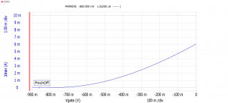
I found that there is a common mistake, made by me too, that Pinch-Off means that the current is pinched-Off to near zero. This not the case, Pinch-Off means that the JFET channel is pinched off. AT pinch off if the Drain voltage is increased the pinched off channel will shorten a little, the resistance will increase a little and the current will remain constant, this dynamic is said to be “Saturated”. So when the Gate Voltage is equal to Vp (Pinch-Off Voltage), (1-Vgs/Vp)^2=0 and Id = Idss.
Pinch-Off is the point that separates the ohmic part of the curve from the saturated part of the curve.
Thanks DT
Oops.
I started working on the challenge, conceptually testing my definitions and assumptions, you know a reality check.
I found that there is a common mistake, made by me too, that Pinch-Off means that the current is pinched-Off to near zero. This not the case, Pinch-Off means that the JFET channel is pinched off. AT pinch off if the Drain voltage is increased the pinched off channel will shorten a little, the resistance will increase a little and the current will remain constant, this dynamic is said to be “Saturated”. So when the Gate Voltage is equal to Vp (Pinch-Off Voltage), (1-Vgs/Vp)^2=0 and Id = Idss.
Pinch-Off is the point that separates the ohmic part of the curve from the saturated part of the curve.
Thanks DT
Attachments
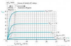
There's a theoretical Vpo.
Actual current never gets to ZERO because there is sub-threshold conduction.
The sub-threshold current is too small to measure in production. All datasheets say what "small" current defines the published Vgs('off') measurement.
Indeed if you want a "true" Vpo you should extrapolate the curve from higher currents.
If you are not going to work the JFET near-OFF, then the actual or theoretical value of Vgs(off) is not much use. Comparing similar JFETs it is convenient to just use a 1Meg source resistor (~~few-uA current).
- Status
- This old topic is closed. If you want to reopen this topic, contact a moderator using the "Report Post" button.
- Home
- Amplifiers
- Pass Labs
- JFET Matching/Sorting