Thanks Mr. Pass. BestAt the moment I do not have plans to sell those boards.

buzzforb: The last picture in the sixmoons article showed with good clarity the inside of Mr. Pass's F6. It is a goldmine of info for the DIYer. Suppose that he used an industry standard enclosure. The long side of the PCBs is along its known depth dimension. One can calculate/estimate the minimum distance between the center of the power toroid and the edges of the JENSEN closest to it for no hum. One can also calculate/estimate the center to center distance between the power JFETs for optimal heat distribution on the heat sinks.Do we hav eto worry abou tproximity to toroid considering use of xformer? In my rats nest, i ha dto keep some diatance from toroid to prevent little hum. Most likely rats nest, bu tthough ti would ask. Also, i notice that Nelson shoves his all the way in the back, away from the main doughnut.
There are 5 power resistors [ big and light grey] on each PCB. By comparison, the schematic showed only 2; and here I speculate they belong to the feedback loop. I'll gaze more at the PCBs and understand what's it mean if anything.
Based on their location it looks like there are two 3 watt source resistors per JFET and one 3 watt resistor for each feeback loop. I suspect that the 2 resistors in parallel per JFET are in order to tune the resistance. Papa probably has two sets of resistances on rotary switches for adjusting a channel, and then solders resistors into the board to match. Anyway, that is how I would do it for production.
buzzforb: The last picture in the sixmoons article showed with good clarity the inside of Mr. Pass's F6. It is a goldmine of info for the DIYer. Suppose that he used an industry standard enclosure. The long side of the PCBs is along its known depth dimension. One can calculate/estimate the minimum distance between the center of the power toroid and the edges of the JENSEN closest to it for no hum. One can also calculate/estimate the center to center distance between the power JFETs for optimal heat distribution on the heat sinks.
There are 5 power resistors [ big and light grey] on each PCB. By comparison, the schematic showed only 2; and here I speculate they belong to the feedback loop. I'll gaze more at the PCBs and understand what's it mean if anything.
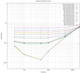
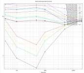
Here are some interesting plots based on Spice simulations with combinations of Rs1 and the Rs2, the upper and lower source resistors respectively. In all cases the F6 is driving an 8 ohm load at 1 watt. The plots are of the harmonics H2, H3 and H2/H3.
Attachments
Thanks lhquam. I am still missing the 100 Ohm/5W for the feedback loop. One clearly sees the 20 Ohmer to ground. One also sees two electrolytic capacitors [of similar physical size] per JFET. Maybe two 470 uF in parallel adding up to the prescribed 1,000 uF of the schematic? The low wattage resistor between each pair of these electrolytics is the 10K resistor connected to the wiper of the 5K bias pot.Based on their location it looks like there are two 3 watt source resistors per JFET and one 3 watt resistor for each feeback loop. I suspect that the 2 resistors in parallel per JFET are in order to tune the resistance. Papa probably has two sets of resistances on rotary switches for adjusting a channel, and then solders resistors into the board to match. Anyway, that is how I would do it for production.
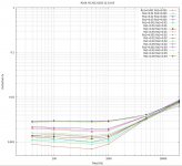
Simulation vs Measurements
For those of you who are sceptical about the utility of Spice simulations, particularly when transformers are involved, here are two plots that show a reasonable degree of agreement between simulation and measurement.
The plots show THD, H2, H2, H2phase, and H3 phase. The upper plot is from simulation; the lower plot from actual measurement of the Teaser-6 left channel.
Attachments
Based on their location it looks like there are two 3 watt source resistors per JFET and one 3 watt resistor for each feeback loop. I suspect that the 2 resistors in parallel per JFET are in order to tune the resistance. Papa probably has two sets of resistances on rotary switches for adjusting a channel, and then solders resistors into the board to match. Anyway, that is how I would do it for production.
It confirms the obivious that Nelson tunes his amplifier to ear and measurement, and not a given schematic, much like Ilquam has done with all his work . No magic, just measuring, listening, and adjusting.
Here are some interesting plots based on Spice simulations with combinations of Rs1 and the Rs2, the upper and lower source resistors respectively. In all cases the F6 is driving an 8 ohm load at 1 watt. The plots are of the harmonics H2, H3 and H2/H3.
Could you explain the 3rd simulation, H2/H3. The scale starts at 1% and goes off the chart?
Rush
The scale is not %, but the ratio of H2 to H3. Yes, one of the plots goes off the chart - I just got overzealous in windowing the graph.
Could you explain the 3rd simulation, H2/H3. The scale starts at 1% and goes off the chart?
Rush
I measured the hum & noise on my Teaser-6 with a Fluke meter. Outputs connected to 8 ohm loads. Inputs connected to M-Audio AP-192 sound card with no signal.
left channel: 0.6mV AC RMS
right channel: 0.2mV AC RMS
As shown in post #1519 http://www.diyaudio.com/forums/pass-labs/216616-f6-amplifier-152.html#post3157489, the left channel is much closer to the toroid. However, not all the difference is due to the coupling to the Jensen transformers. I saw similar (but smaller) differences with a pair of F5 channels using the same heatsink and chassis.
http://www.diyaudio.com/forums/pass-labs/216616-f6-amplifier-152.html#post3157489
Based on their location it looks like there are two 3 watt source resistors per JFET and one 3 watt resistor for each feedback loop.
You will want to recall in the talk that this photo was taken early in the process...
I am still trying to understand the effect of the output resistors
I went back to the .1ohm/10ohm pot combo and noticed the following when I run the pot through its 15 turns. The resistance on my DMM starts at .3 ohms rises to 3ohms and then falls to .4 ohms. It does this whether I am measuring from wiper to either side of pot. I understand that my DMM does not measure milliohms but I did not expect this behavior. I am assuming it is some kind of artifact.
I think somebody mentioned earlier in this thread using rotary switches to load the source of the output JFet. More of a pain to put together but for each JFet would a rotary switch with 0 ohms, 2x .025 ohms in parallel,.025 ohms, 1x .025 and 1x .1 ohms in parallel, .05 ohms, .025 ohms +.05 ohms in series, and .1 ohms. This would give a switch with 0, .0125, .025, .033, .05, .075 and 1 ohms.
Overkill? At least I would know load resistance.
Thoughts
Thanks
Bob
The pictures of the device in the 6moons article gave the impression it was a prototype. No power switch on the front panel, it sat on an active workbench, and the wiring at the rear panel appeared to be work or testing in progress.You will want to recall in the talk that this photo was taken early in the process...
I am still trying to understand the effect of the output resistors
I went back to the .1ohm/10ohm pot combo and noticed the following when I run the pot through its 15 turns......
Bob
that's logical
but - do not forget that ZAP is voltage divider there , so , you're having 0-100% voltage for degeneration purpose , of whatever source resistance it is
from buzzforb
I will probably botch this, but the pot can only minimize the effect of the Rs, not increase it.
from ZenMod
but - do not forget that ZAP is voltage divider there , so , you're having 0-100% voltage for degeneration purpose , of whatever source resistance it is
You guys are, of course, right. For .1 ohms it should be 0 to .099xx or .1ohms.
Probably should just accept I can't measure it with my equipment. Maybe its time to bight the bullet and learn how to measure distortion. A number of you have mentioned Electroacoustics Toolbox and they do have a demo version.
Best
Here is an LTSpice simulation of the F6 using IRFP240 fets, and "tuning the Zen pot to keep the ratio H2/H3 approximately constant. I estimate the transconductance of the IRFP at 1.4A bias to be 3.5S.
This looks pretty good. I need to build it and see how it measures and sounds.
Has anyone thought out the value of R1 to keep relative gain at 15db if using IRFP240's? I am prototyping this, but uncertain of a formula that can help.
My apologies if this has been mentioned already. I assume tweaking this and the degeneration resistors will get this working on point. I plan on using for source resistors 1R to start with the 10R Zen Pots.
- Home
- Amplifiers
- Pass Labs
- F6 Amplifier