
With the adjustments made in post #1889 http://www.diyaudio.com/forums/pass-labs/216616-f6-amplifier-189.html#post3166398, the sound is much improved. After listening for an evening, I am getting much happier with this amp. I still have one channel that isn't so good that I am working on. I do not know if the problem is with the output R100s, the xformer, or something else. As soon as both channels are performing well I can declare victory.
Is this thread going/gone quiet [globally]? A lot of subjective, objective knowledge and learning has been accomplished [and taught] todate by lhquam, buzzforb, Zen Mod and countless other DIYers. lhquam; Did you reach your destination and achieve your goals?
I do not know if the problem is with the output R100s said:I thought it was clearly the R100s when you swapped them.
Something new makes you hesitate?
You are right  about the problem moving with the R100's. While I have the boards off of the amp right now, I think I will remove the R100's and measure their transconductance and a few other parameters. I expect delivery of additional R100s tomorrow. I will solder in some 3-pin Molex sockets to make the exchange of output FETs easier.
about the problem moving with the R100's. While I have the boards off of the amp right now, I think I will remove the R100's and measure their transconductance and a few other parameters. I expect delivery of additional R100s tomorrow. I will solder in some 3-pin Molex sockets to make the exchange of output FETs easier.I thought it was clearly the R100s when you swapped them.
Something new makes you hesitate?
With the adjustments made in post #1889 http://www.diyaudio.com/forums/pass-labs/216616-f6-amplifier-189.html#post3166398, the sound is much improved. After listening for an evening, I am getting much happier with this amp. I still have one channel that isn't so good that I am working on. I do not know if the problem is with the output R100s, the xformer, or something else. As soon as both channels are performing well I can declare victory.
In the interim, consider the following longer range proposal. Mr. Pass has created a classic power amp himself using his inventive topology named STASIS {R} while with/at Threshold Corporation. The attendant United States Patent #4,107,619 was granted on Aug. 15, 1978. You may wish to tackle this new mission. Simplify, infuse and refurbish this classic design with new technology active/passive devices and know-how like Mr Pass has done with F6.
I made the in-circuit measurement of the R100 transconductances of PBC1 and got 6.3S for the upper FET and 7.5S for the lower FET. Since the source resistors have 5% tolerances, the calculation has corresponding uncertainty.
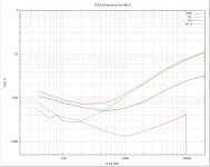
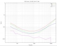
Here are plots of the two channels adjusted for the best nulling of the 2nd harmonic in the mid frequencies. The first plot is from PCB1 (with the poorer measurements). The second plot is from PCB2 (the better channel). I would expect to be able to do a better job of nulling the 2nd harmonics for PCB1.
Here are plots of the two channels adjusted for the best nulling of the 2nd harmonic in the mid frequencies. The first plot is from PCB1 (with the poorer measurements). The second plot is from PCB2 (the better channel). I would expect to be able to do a better job of nulling the 2nd harmonics for PCB1.
You don't need to remove the R100's, just measure the AC voltage Gate
to Source and compare it to the AC voltage across the source resistance.
At 100 Hz, a cheap ac voltmeter will do it.

Attachments
Last edited:
If true, then we still have a lot of work to do. I either missed that post or totally forgot about it.
I have not found SemiSouth data on the SOA (safe operating area) for the R100. Vds does not appear to an issue. The problem is power dissipation vs. heatsink temperature. The only R100 datasheet spec is 144W max at 25C. Not very helpful.
I would assume 45-48 volt rails and parallel R100s would be needed, requiring larger source resistors than 0R12. More transconductance from parallel FETs, but less transconductance per FET.
It doesn't look like the front end or bias circuitry would need to change.
Thanks for bringing it up. Scaling up the F6 is something some might consider.
The post is 5 years old, but it is an interesting twist.
Except for the F5T, it goes outside the FW philosophy, e.I., low Watts.
I just found an updated SemiSouth R100 datasheet that contains the SOA. http://semisouth.com/wp-content/uploads/2011/05/SJEP120R100.pdf I still do not see info about max power dissipation vs. temperature.
If true, then we still have a lot of work to do. I either missed that post or totally forgot about it.
I have not found SemiSouth data on the SOA (safe operating area) for the R100. Vds does not appear to an issue. The problem is power dissipation vs. heatsink temperature. The only R100 datasheet spec is 144W max at 25C. Not very helpful.
I would assume 45-48 volt rails and parallel R100s would be needed, requiring larger source resistors than 0R12. More transconductance from parallel FETs, but less transconductance per FET.
It doesn't look like the front end or bias circuitry would need to change.
- Home
- Amplifiers
- Pass Labs
- F6 Amplifier