Ah, it was originally for 4v biasing.
About 10k instead of 3.32k.
Or lower voltage zenners.
I would imagine if executed with SemiSouth's you need no more than 2V for conduction.
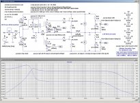
Here is an update of my schematic and its Bode plot. You should note the 2 pole RC filter supplying the bias voltage for the upper output FET. This significantly improves the low frequency THD. The high frequency response shown agrees well with actual measurements. I cannot really test the low frequency rolloff. This implementation does not suffer from the low frequency oscillation problem that my previous build exhibited.
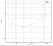
Also shown it the THD plot of the rewired circuit. It is interesting to note the at low frequencies the 3rd harmonic dominates; at high frequencies the 2nd harmonic dominates. The crossover it at about 700 Hz. (I really need to do a Bode plot of the harmonics separately.)
Also shown it the THD plot of the rewired circuit. It is interesting to note the at low frequencies the 3rd harmonic dominates; at high frequencies the 2nd harmonic dominates. The crossover it at about 700 Hz. (I really need to do a Bode plot of the harmonics separately.)
Attachments
And you do not need to adjust below 1v to 1.2v.I would imagine if executed with SemiSouth's you need no more than 2V for conduction.
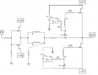
You show the realtionship between V- and the lower bias circuit to be identical to the relationship between Vo and the upper bias circuit. Will this shown high symmetry give a highly symmetrical performance before loop feedback?Same as previous but with corrected values.
Same as previous but with corrected values.
now choose Rs value & Iq , and calculate that in

ZM will allow at least 1mA through trimpot , and 3mA through zenner
in fact - ZM will use two 3mm greenies (meaning 2x1V93@3-5mA) in series instead - more shiny

and , after that ,ZM will use CCS-es - feeding voltage references , just for fun
why simple , when it can be complicated

Last edited:
Here is an update of my schematic and its Bode plot. You should note the 2 pole RC filter supplying the bias voltage for the upper output FET. This significantly improves the low frequency THD. The high frequency response shown agrees well with actual measurements. I cannot really test the low frequency rolloff. This implementation does not suffer from the low frequency oscillation problem that my previous build exhibited.
Also shown it the THD plot of the rewired circuit. It is interesting to note the at low frequencies the 3rd harmonic dominates; at high frequencies the 2nd harmonic dominates. The crossover it at about 700 Hz. (I really need to do a Bode plot of the harmonics separately.)
lhquam: Your refined circuit like its parent still has the following observations:
- The capacitor connected to the lead of the bottom transformer [circle] a dead short to AC ground [or V-] under all operating conditions.
- The lead of the transformer's upper winding [no circle] which is connected to a same-valued capacitor is not [never] at AC ground. The impedance from this upper transformer aiming at ground is the sum of the resistances and through the upper bias regulator to its official ground.
If one insists on exact matching, then the answer maybe found [or not] in the schematics of the old classic parent[ with bjts] of Conceptual F6.
Would you consider simulating the old classic design using LTSPICE as a comparative reference?
How about this?
hell , no ;
CCS instead of 6k8 resistor(s) , in bobbo's sch
you'll make a big badaboom with sch in your pdf
No, regs for bias and maybe FE. If 2 pole filter on bias circuit improved LF distortion, doesnt that suggest riplle/noise is getting through simple RC and causing distortion.
see - zener is already reg ........... (shunt one )
LED also .........
feeding it with CCS is just making it better
audibly better - probably not
but , I can't resist - Babelfishing is my hobby
That is direct copy of Vref off of Salas shunt in DCB1.
still big badaboom
you need to change places of leds and CCS
I am not sure what the relevance is for "AC ground". What is important are the bias voltages relative to the bottom of the FET source resistors. We are trying to maintain these voltages at constant levels under varying signal conditions.
lhquam: Your refined circuit like its parent still has the following observations:
Like the schematic of bobodioulasso which shares the identical observations, it is apparently difficult to exactly match the input circuits of the upper and lower JFETs.
- The capacitor connected to the lead of the bottom transformer [circle] a dead short to AC ground [or V-] under all operating conditions.
- The lead of the transformer's upper winding [no circle] which is connected to a same-valued capacitor is not [never] at AC ground. The impedance from this upper transformer aiming at ground is the sum of the resistances and through the upper bias regulator to its official ground.
If one insists on exact matching, then the answer maybe found [or not] in the schematics of the old classic parent[ with bjts] of Conceptual F6.
Would you consider simulating the old classic design using LTSPICE as a comparative reference?

- Home
- Amplifiers
- Pass Labs
- F6 Amplifier