You might note that there was considerable discussion of "Bias Method B" vs Bias Method A" back in post #742. http://www.diyaudio.com/forums/pass-labs/216616-f6-amplifier-75.html#post3124507 Zen Mod steered me away from method B which is the one you just presented.I took the time this morning to review my history of posts in this thread,
and I conclude that you would benefit from some additional information.
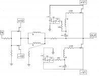
Notice the particular placement of capacitors, resistors, and transformer
secondaries which give greater output DC offset stability without
sacrificing the symmetry of the two halves at AC.

Method B is acceptable on the negative half of the circuit. Bias voltage
referenced to ground is preferred on the positive half.
The issue is whether the difference in loading presented by the high
impedance bias resistor is different enough to affect the symmetry of the
drive.
On the positive half, the bias resistor sees the output swing, which loads
the secondary more than on the negative side, where it sees a constant
value.
The arrangement I use has the bias voltage bootstrapped by the Source
voltage through the capacitor, so that the difference in loading is
negligible.
Of course, as pointed out previously, this presumes perfect symmetry as
the goal.
And of course you are still free to otherwise load the secondary arbitrarily
for adjustment of the open loop response of the transformer. My
experience was that it did not need adjustment.
There could be dangers in having the capacitor Cb and biasing resistor Rb too high.I took the time this morning to review my history of posts in this thread,
and I conclude that you would benefit from some additional information.
Notice the particular placement of capacitors, resistors, and transformer
secondaries which give greater output DC offset stability without
sacrificing the symmetry of the two halves at AC.
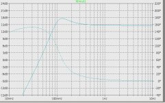
The first graph is a Bode plot for Cb=220uf and Rb=100k. You should note that the phase margin is about 150 degrees, meaning it will oscillate at around .1 Hz. I have observed such low frequency oscillations.
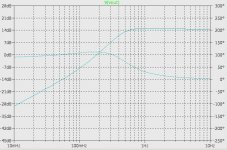
The second graph is Bode plot for Cb=22uf and Rb=47k. The phase margin is about 110 degrees. This will not oscillate, and should not degrade the low frequency performance of the amplifier.
Attachments
I took the time this morning to review my history of posts in this thread,
and I conclude that you would benefit from some additional information.
Notice the particular placement of capacitors, resistors, and transformer
secondaries which give greater output DC offset stability without
sacrificing the symmetry of the two halves at AC.
Thank you !!
There could be dangers in having the capacitor Cb and biasing resistor Rb too high.
As a practical matter, you won't have Rb values of 100K due to the
Gate leakage figures of the Jfets. The 10K range is a more likely value.

The only DC thru the coils is gate leakage currents of around 2uA. No big deal.We can see no DC blocking caps are used (according to original schematic).
Dc through the coils are opposite directions and their effect on the core of the transformer are cancelling eachother.
but that biasing scheme is flawed in few things more ;
you really need to have stable bias ref voltage (either voltage reference or resistor bypassed wit cap ) , then biasing net must be connected to modulating point through resistor of some higher value
as I wrote previously - last few Pa's articles (simple amps ) , same as BA1 FE detail are enough
Thanks zm, had a look at the ba1 - and yup the Zener+var r looks like it will do the trick nicely ! Cheers
lhquam: you wrote above:
"The first graph is a Bode plot for Cb=220uf and Rb=100k. You should note that the phase margin is about 150 degrees, meaning it will oscillate at around .1 Hz. I have observed such low frequency oscillations."
Suppose Rb of the upper bias circuit is replaced by a lower value resistor in series with a forward biased small signal switching diode. At idle, both of the upper and lower capacitors [post #1096] are fully charged. This diode switches off and isolates its upper capacitor from ground at a certain output voltage due to its reverse bias. From this point upward, the upper JFET operates on the stored charge of its bootstrapped capacitor [to Vo] of high value. As the output voltage returns to the value of ground, this upper capacitor is recharged as the switching diode resumes its forward bias.
A 10K value for Rb or even lower, and an optional switching diode in series with it; if this diode adds value to the operation of the upper JFET.I believe Nelson suggested 10K. Why not run with it?
Last edited:
Sticking with Ba 1 voltage source?
Does it matter that you have +/- 12k to ground on the upper gate and +/- 21k to ground on lower gate?
It seems to me that it would reflect a different impedance back, loosing some balance?
Rush
Attachments

Sticking with Ba 1 voltage source?
just recalculate values , so you don't have too great voltage span at trimpot
Rush: Tentatively, the underlined [or asymmetry] may be beneficial. First you control it to any extent you need. Secondly, Mr. Pass wrote in one his numerous publications [and I am paraphrasing very loosely] that a music signal is intrinsically asymmetric [or needs to be]. He found that the absolute magnitude of the positive going signal is larger in value than the negative portion of the same signal. I vaguely recall a significant imbalance of 5-10%. I hope that Mr. Pass corrects my statement for accuracy, and he or other luminaries find the actual excerpt including its context, and reproduce it verbatim in an upcoming post. And further, clarify the value [if any] of a deliberate imbalance to the upper JFET.Does it matter that you have +/- 12k to ground on the upper gate and +/- 21k to ground on lower gate?
It seems to me that it would reflect a different impedance back, loosing some balance?
Rush
If this shoe fits, then accept this "miniscule" underlined imbalance as most probably beneficial to music enjoyment; says mother nature.
Last edited:
- Home
- Amplifiers
- Pass Labs
- F6 Amplifier