on a completely different note - has anyone figured out yet why two voltage rails for output stage vs input stage ? It can't be something trivial given that they are shown as distinct in the simplified schematic. Any clues anyone ?
Mr. Pass, maybe throw us a bone or two ?") )
)
Mr. Pass, maybe throw us a bone or two ?
)EXCELLENT QUESTIONon a completely different note - has anyone figured out yet why two voltage rails for output stage vs input stage ? It can't be something trivial given that they are shown as distinct in the simplified schematic. Any clues anyone ?
Mr. Pass, maybe throw us a bone or two ?
My initial guess was that the input stage rails are reduced to limit power dissipation on the input JFETs. But, knowing the devious nature of our Papa guru, I am now thinking otherwise.
Could the 2 supplies be floating relative to one another in circlotron fashion? The transformer would facilitate that, but the feedback would be different than shown. Perhaps he devised a different way to make a truly symmetrical amplifier from N channel only JFETs that is not a circlotron.
That would mean that I have been on a wild goose chase with my design. Not a total loss, since I have learned a few things along the way.
Last edited:
triode_ al: I like [and hopefully others will appreciate] your schematic in post #1023 because:
- The bias to the upper MOSFET is referenced to the output and not to ground. Thus; this MOSFET will always operate Class A. By contrast, lhquam has the corresponding bias in his prototype referenced instead to ground.
- The bias to the upper MOSFET is [hopefully] stable due to the CCS you used to establish it. I would have used [on paper] an independent power supply of positive voltage higher than the rail voltage shown. Bias in this newer instance will be granite solid or better. By comparison, kasey197, uses a resistor voltage divider to establish bias in his prototype. It may suffice. But; it may also appear to be less robust [rock stable] than the one you are using.
- The bias to the bottom MOSFET can be anything else that is stable; which you do show, and others do.
- The blocking capacitors in series with the gates of the MOSFETs eliminate the dreaded direct current through the secondaries.
re
- The bias is like the conceptual scheme:

It is attached to the output where the voltage across the xfrm is 0. A cap does the same in a different layout.
Yes, I could use a bootstrap to the power supply of the CCS of the top circuit. Is a good idea. But that implies I use the same time constant in all 4 bias circuits (or else - I have huge bumps, worse than goose bumps).
CCS (near-contant current) is different from near-constant voltage like Kasey does, but the effect can be the same, only my bias is adjustable and I like to be able to set the current like in the F5 - to manage the output zero.
I do have a separate PS for the input buffer, running at +/- 35V and that leaves enough headroom for the bias so I won't have troubles in minor shifts in the CCS.
Floating V1 supply concept
Note that if you move V2 to between J2 and Out+ you have a circlotron.
Here is an idea of the circlotron-like amplifier. Feedback uses the 4th transformer coil.on a completely different note - has anyone figured out yet why two voltage rails for output stage vs input stage ? It can't be something trivial given that they are shown as distinct in the simplified schematic. Any clues anyone ?
Mr. Pass, maybe throw us a bone or two ?
Note that if you move V2 to between J2 and Out+ you have a circlotron.
Attachments
Last edited:
In trying to determine the ideal load resistor for the transformer, does the circuit need to be complete including output stage or can it be determined with just the transformer connected to the input stage?
complete
tell me which sch you are going to use , and I'll tell you what part you need to vary
complete
tell me which sch you are going to use , and I'll tell you what part you need to vary
I am going to try multiple, but had intended to start with b1 bias schema. Ill draw it up like i got it wired. Hopefully it wont blow up. Just to be stubborn, i am going to trywith secondaries wired in phase. The SILENCER sounds really cool, and i need to learn anyway.
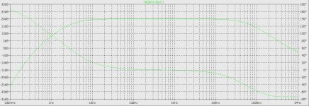
I did a Spice simulation of this idea but the high frequency response was bad. The response is down 3dB at about 10kHz. I tried a variety of different impedances for the feedback network.Here is an idea of the circlotron-like amplifier. Feedback uses the 4th transformer coil.
Note that if you move V2 to between J2 and Out+ you have a circlotron.
I did a Spice simulation of this idea but the high frequency response was bad. The response is down 3dB at about 10kHz. I tried a variety of different impedances for the feedback network.
Why burden your circuit with negative feedback? Without NFB, the output stage is Circlotronic, has high power [value?], and low distortion [value?]. What else are you seeking? Most probably you'll say a low output impedance; but where will its physical location be ? Will the low output impedance be at the junction of the power supplies and/or the joint between the source of upper JFET and the drain of lower JFET. Your thoughts!
has anyone figured out yet why two voltage rails for output stage vs input stage ?
I am making an allowance for dissipation ratings of the input Jfets. Their
bias figure is not degenerated, so with some devices the current can get
pretty high. Also, this design can be run at higher rail voltages, maybe too
high for those inputs.
You will see my answer soon. Circlotrons work with or without negative feedback, your choice.Why burden your circuit with negative feedback? Without NFB, the output stage is Circlotronic, has high power [value?], and low distortion [value?]. What else are you seeking? Most probably you'll say a low output impedance; but where will its physical location be ? Will the low output impedance be at the junction of the power supplies and/or the joint between the source of upper JFET and the drain of lower JFET. Your thoughts!
First, I agree with Ihquam. As Papa has said, driving these transformers takes the lowest output Z for best results. Of coarse exactly what your trying to do is important also... for the complementary buffer to have the lowest output impeadance, you would want to use the Highest IDss parts you can. Some may argue but, that will ussually mean the highest transconductance. That will create the lowest output Z. If you are selecting 10mA or higher Idss parts, you probably want to keep the voltage down and the /part Pd to 100-120mW.on a completely different note - has anyone figured out yet why two voltage rails for output stage vs input stage ? It can't be something trivial given that they are shown as distinct in the simplified schematic. Any clues anyone ?
Mr. Pass, maybe throw us a bone or two ?
This low output Z thing is passed through the transformer (sometimes said to be reflected) to generate a source impeadance that drives the output FETs. The function is Buffer out Z * turns ratio^2 = Secondary output Z or the source impeadance the FETs sees.
Guess I'm a little late??
Your circuit is special. I am glad you continue to unravel its potential.You will see my answer soon. Circlotrons work with or without negative feedback, your choice.
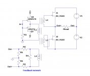
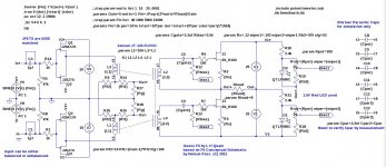
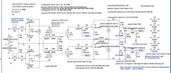
Balanced F6
Here is an F6 design that is fully symmetric in the spirit of a circlotron. The output power supplies float relative to ground, but not relative to each other. The harmonic distortion is primarily 3rd order. It will accept either balanced or unbalanced inputs.
I have simulated it with LTSpice and it looks very good.
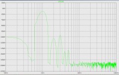
The power spectrum plot in for 1 watt output at 1kHz into 8 ohms.
Here is an F6 design that is fully symmetric in the spirit of a circlotron. The output power supplies float relative to ground, but not relative to each other. The harmonic distortion is primarily 3rd order. It will accept either balanced or unbalanced inputs.
I have simulated it with LTSpice and it looks very good.
The power spectrum plot in for 1 watt output at 1kHz into 8 ohms.
Attachments
How do you control offset? A pot will have a degenerative effect, correct.I am making an allowance for dissipation ratings of the input Jfets. Their
bias figure is not degenerated, so with some devices the current can get
pretty high. Also, this design can be run at higher rail voltages, maybe too
high for those inputs.
Whao; you have a creative development. Is the underlined mean that your circuit satisfies the requirements of a "genuine" Circlotron?Here is an F6 design that is fully symmetric in the spirit of a circlotron. The output power supplies float relative to ground, but not relative to each other. The harmonic distortion is primarily 3rd order. It will accept either balanced or unbalanced inputs.
I have simulated it with LTSpice and it looks very good.
The power spectrum plot in for 1 watt output at 1kHz into 8 ohms.
How do you control offset?
I reference the positive half DC values to ground.
The only difference from a circlotron that I know about is the position of the power supply V1 relative to the output FET.Whao; you have a creative development. Is the underlined mean that your circuit satisfies the requirements of a "genuine" Circlotron?
- In my circuit, there is the clockwise loop: Rload - V1 - R4 - J3
- In a circlotron the loop is: Rload - R4 - J3 - V1
Like this?I reference the positive half DC values to ground.
Attachments
- Home
- Amplifiers
- Pass Labs
- F6 Amplifier