Perhaps this would be of interest to some.
http://www.diyaudio.com/forums/solid-state/24744-push-pull-using-only-n-channel-mosfets.html
It introduces a new problem to consider...offset control.
http://www.diyaudio.com/forums/solid-state/24744-push-pull-using-only-n-channel-mosfets.html
It introduces a new problem to consider...offset control.
Perhaps this would be of interest to some.
http://www.diyaudio.com/forums/solid-state/24744-push-pull-using-only-n-channel-mosfets.html
It introduces a new problem to consider...offset control.[/QUOTE]
Interesting schematic in the link above. It shows a step-down transformer [4:1], and a capacitor in series with the secondary winding to block dc emanating from the simple resistor string divider used for bias.
The underlined may suggest using an output capacitor to block dangerous [to the load] levels. Is there a reason against using a mono-polar power supply [and thus a blocking output capacitor like in OTLAmp1] instead of a split + and - voltage rails? Some of the amps by Mr. Pass use output blocking caps; e.g. the recent ACA#1.

Thank you Loudthud for your interesting analysis. It, and that of flg earlier now suggest that the upper FET is simply [and only] working as a modulated current source load to the bottom FET which is the [only] voltage gain device. Thus the math expression ZM used earlier relating voltage gain to the [bottom] FET's transconductance and load fits. This working scenario is palatable and digestible. I am happy.
As I see it both output FETS are voltage amplifiers.
- The Xfmr generates a current in both devices in opposite phase.
- Because they float, and the top one, not having a load on the Drain and not having a fixed Source, will dump the current that is being 'generated' by the gate modulation into the common out.
- Both sides do that in parallel. . .
- Without feedback, it is extreme high impedance.
triode_al: I agree with you regarding the underlined, and the bullet items; but I am not sure about the last one on the extreme high impedance. Please refer to post #679 which is my newer understanding of the operation of the output stage of Conceptual F6. This understanding led me to propose a model shown in post #769, and a new thread which is entitled "Compound Power Amplifiers" in the Pass Labs Forum. The upper JFET is a voltage source amplifier [VSA] with gain. Its output current gain multiplied by the value of the load resistor is simplistically its voltage gain. It is universally accepted that the emitter port of a bjt, and the source port of a FET are intrinsically low impedance. Low is a relative term. The lower JFET is a current source amp or a transconductance amp [TCA]. It is also universally accepted that the collector of bjt and the drain of FET are high impedance ports. The output current gain of the lower JFET multiplied by the value of the load resistor is simplistically its voltage gain. The voltage gain from the upper JFET is equal to the voltage gain of the lower JFET; because of strict matching of the drive signals, and the JFETs. Thus; neither JFET drives current into the other. Each one appears as a very high impedance to the other; an impedance which is much higher than the value of the load resistor. So,their output voltage drives current only through the load.As I see it both output FETS are voltage amplifiers.
- The Xfmr generates a current in both devices in opposite phase.
- Because they float, and the top one, not having a load on the Drain and not having a fixed Source, will dump the current that is being 'generated' by the gate modulation into the common out.
- Both sides do that in parallel. . .
- Without feedback, it is extreme high impedance.
The low output impedance [due only to the upper JFET] is then lowered further with loop feedback.
As I see it both output FETS are voltage amplifiers.
Operating Common-Source, they are both voltage and current amplifiers.

Thank you for the clarification.Operating Common-Source, they are both voltage and current amplifiers.
Operating Common-Source, they are both voltage and current amplifiers.
If drawn with the PSU, dont we see that both fets are passing signals through the PSU to the load, sort of like a circlotron. That is why Kasey got double the gain of what a single fet would yield
Getting close
I think I have found a simple and very stable bias circuit for the F6.
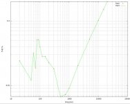
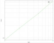
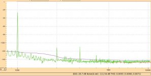
I wired it up and made measurements. From 500Hz to 20KHz the THD behaves as one would expect. Below 500Hz, the THD increases in a highly erratic manner. See the figures below.
All tests were with 8 ohm load, 1.3A bias and 25V rails.
The frequency sweep is at 1 watt.
The power sweep is at 1kHz.
The spectrum is at 1kHz and 1 watt.
I am temporarily withholding the schematic so that I do not spoil your fun.
I think I have found a simple and very stable bias circuit for the F6.
I wired it up and made measurements. From 500Hz to 20KHz the THD behaves as one would expect. Below 500Hz, the THD increases in a highly erratic manner. See the figures below.
All tests were with 8 ohm load, 1.3A bias and 25V rails.
The frequency sweep is at 1 watt.
The power sweep is at 1kHz.
The spectrum is at 1kHz and 1 watt.
I am temporarily withholding the schematic so that I do not spoil your fun.
Attachments
If drawn with the PSU, dont we see that both fets are passing signals through the PSU to the load, sort of like a circlotron. That is why Kasey got double the gain of what a single fet would yield
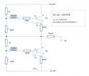
buzzforb: I hope that I put your words above in 3 simplified schematics of the attached file. Fig. 1 shows the direction of current flow [Io] through the load from the upper JFET only due to a positive signal at its gate. Fig. 2 shows the direction of current flow [Io] through the same load from the bottom JFET only due to the remaining [inverted] portion of the sine signal at its gate. Fig. 3 shows the integrated current through the load from the contribution of the upper JFET [shaded positive part of sine] and the contribution of the lower JFET [unshaded negative]. Its net value= 2Io. The net voltage across the load Zl is equal to 2Io multiplied by Zl.
Attachments
Last edited:
Kasey197 or others,
Is bias stablity an issue with the simple R divider version?
Not for me ... but both types of fets I tried had a postive tempco (2sk1058 and SS R100s). I presume with vertical fets IRF etc youd have to add a tehrmistor to keep things well managed but never tried it (beyond frying a pair of IRFs in complementary pp)
I think I have found a simple and very stable bias circuit for the F6.
I wired it up and made measurements. From 500Hz to 20KHz the THD behaves as one would expect. Below 500Hz, the THD increases in a highly erratic manner. See the figures below.
All tests were with 8 ohm load, 1.3A bias and 25V rails.
The frequency sweep is at 1 watt.
The power sweep is at 1kHz.
The spectrum is at 1kHz and 1 watt.
I am temporarily withholding the schematic so that I do not spoil your fun.
Well done !!
How much was the gain of the complete circuit ? Im assuming your tx is set up is 1:1 right ? Edit: Also if/when you get a chance, what was the output impedance you found ?
Last edited:
ZM, lhquam and others... I am wondering what i'm missing regarding the DC through the coils issue.
I'm using this approach at the moment and tried measuring the DC current thru the coils but couldn't get anything. Was wondering if i'm oversimplifying things in my head or perhaps the current starts to appear in some cases which I haven't tested for ? Eg maybe if driving the fets >3V with SS R100s in output etc ?
Just want to make sure I understand before I order some nice input txs
Cheers all,
Attachments
Operating Common-Source, they are both voltage and current amplifiers.
Antionel,
I could be totally wrong, but I was considering this if both fets are seeing the same signal.
KAsey,
What is preventing DC through the coils? Doesnt the coil see the DC bias for the fet or is your cap stopping that?
Attachments
Last edited:
The closed-loop gain was slightly less than 6x, using 50 ohms and 10 ohms for the feedback divider. Tx is 1:1, both primaries in parallel. I haven't attempted to measure output impedance.Well done !!
How much was the gain of the complete circuit ? Im assuming your tx is set up is 1:1 right ? Edit: Also if/when you get a chance, what was the output impedance you found ?
The closed-loop gain was slightly less than 6x, using 50 ohms and 10 ohms for the feedback divider. Tx is 1:1, both primaries in parallel. I haven't attempted to measure output impedance.
cool thanks!!
ZM, lhquam and others... I am wondering what i'm missing regarding the DC through the coils issue.
I'm using this approach at the moment and tried measuring the DC current thru the coils but couldn't get anything. Was wondering if i'm oversimplifying things in my head or perhaps the current starts to appear in some cases which I haven't tested for ? Eg maybe if driving the fets >3V with SS R100s in output etc ?
Just want to make sure I understand before I order some nice input txs
Cheers all,
You shouldn't need those caps.
The main problem with this circuit is that it is sensitive to rail voltages. If the fluctuate, the bias changes. There will be only a couple of microamps through the coils due to the FET gate leakage. Otherwise there is no DC path. My R100s have Vgs=1.33V at 1.3A.
Last edited:
- Home
- Amplifiers
- Pass Labs
- F6 Amplifier