hi all,
Had time to fire up the iron again this weekend and wanted to run some tests in open loop (ie no NFB/degeneration) to see if i understood things correctly. Here are some observations, theory and then tests for some proof.
Setup:
Same schema as papas front end (just the tx+output stage). Supply rails +\- 24V. Output devices 2sk1058 hitachi latefts. Bias arrangement: 9V batteries with 5K pot to set voltage. The battery and pot bypassed by 220uF caps. Separate bias for top and bottom halves. Bias current set for 1.4A. Transformer was regular torodial power transformer. Stepup ratio approx 4x.
Results:
0.2V pk-pk in, 9.8V pk-pk out. Therefore gain = 49x. Given the tx gives us 4x, that means the fets are giving us approx 12.2X gain.
Theory:
Load R = 6.8R, therefore combined bottom n top half transconductance = 12.2/6.8 = 1.8 Siemens. Each fet therefore gives us 1.8/2 = 0.9 S transconductance. This seems to tie in with what i see from the hitachi datasheets.
Explanation:
Given the above, both top and bottom fets are acting in common source mode (despite the temptation to think about the top half as a source follower providing no voltage gain). If this hypthesis is true then both top and bottom halves provide equal amounts of gain. We can test this easily given the transformer coupling by just bypassing the top and bottom tx secondaries (ie in turn, each fet would see only the bias voltage, but no signal) individually and seeing the effect.
Results:
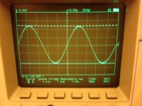
Both secondaries connected, trace 1. Output is 9.8V.
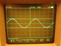
Top secondary bypassed, trace 2,. Output is 4.875V
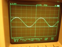
Bottom secondary bypassed, trace 3. Output is 4.812V
Summary: So, the sum of the two halves individually = 9.7V vs 9.8V when theyre both connected. Seems close enough to suggest that the initial hypothesis that both halves act to provide equal amounts of gain (in common source) is correct.
Some other results/thoughts:
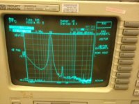
Warts n all open loop, the distortion performance seems pretty remarkable by comparison to a conventional complmenetary push-pull stage built. Here, (trace 4) you can see that theres zilch even harmonics and all were left with is 0.07% THD, almost all of it 3rd harmonic with very little higher order stuff.
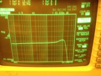
The op stage needs some local feedback so as to reduce the miller effect on input capacitance which is very high. Having said that, the open loop freq response incl tx was quite usefully flat (trace 5). Seems to me that this would run quite respectably as-is w/o nfb if one could live with the HF rolloff and high o/p impedance. Addition of some feedback on this relatively linear stage will make for a pretty nice amp i think.....
Next steps while waiting (for the real F6):
a) Try the same local biasing arrangement i did last time but with lower impedance resistors (need to grab some WW low R pots tom)
b) Build the dual jfet input stage to see how that works....
I'm finding that part of the fun is in the journey .....
Had time to fire up the iron again this weekend and wanted to run some tests in open loop (ie no NFB/degeneration) to see if i understood things correctly. Here are some observations, theory and then tests for some proof.
Setup:
Same schema as papas front end (just the tx+output stage). Supply rails +\- 24V. Output devices 2sk1058 hitachi latefts. Bias arrangement: 9V batteries with 5K pot to set voltage. The battery and pot bypassed by 220uF caps. Separate bias for top and bottom halves. Bias current set for 1.4A. Transformer was regular torodial power transformer. Stepup ratio approx 4x.
Results:
0.2V pk-pk in, 9.8V pk-pk out. Therefore gain = 49x. Given the tx gives us 4x, that means the fets are giving us approx 12.2X gain.
Theory:
Load R = 6.8R, therefore combined bottom n top half transconductance = 12.2/6.8 = 1.8 Siemens. Each fet therefore gives us 1.8/2 = 0.9 S transconductance. This seems to tie in with what i see from the hitachi datasheets.
Explanation:
Given the above, both top and bottom fets are acting in common source mode (despite the temptation to think about the top half as a source follower providing no voltage gain). If this hypthesis is true then both top and bottom halves provide equal amounts of gain. We can test this easily given the transformer coupling by just bypassing the top and bottom tx secondaries (ie in turn, each fet would see only the bias voltage, but no signal) individually and seeing the effect.
Results:
Both secondaries connected, trace 1. Output is 9.8V.
Top secondary bypassed, trace 2,. Output is 4.875V
Bottom secondary bypassed, trace 3. Output is 4.812V
Summary: So, the sum of the two halves individually = 9.7V vs 9.8V when theyre both connected. Seems close enough to suggest that the initial hypothesis that both halves act to provide equal amounts of gain (in common source) is correct.
Some other results/thoughts:
Warts n all open loop, the distortion performance seems pretty remarkable by comparison to a conventional complmenetary push-pull stage built. Here, (trace 4) you can see that theres zilch even harmonics and all were left with is 0.07% THD, almost all of it 3rd harmonic with very little higher order stuff.
The op stage needs some local feedback so as to reduce the miller effect on input capacitance which is very high. Having said that, the open loop freq response incl tx was quite usefully flat (trace 5). Seems to me that this would run quite respectably as-is w/o nfb if one could live with the HF rolloff and high o/p impedance. Addition of some feedback on this relatively linear stage will make for a pretty nice amp i think.....
Next steps while waiting (for the real F6):
a) Try the same local biasing arrangement i did last time but with lower impedance resistors (need to grab some WW low R pots tom)
b) Build the dual jfet input stage to see how that works....
I'm finding that part of the fun is in the journey .....
Attachments
Great work kasey. You've separated [and delivered] fact from fiction.hi all,
Had time to fire up the iron again this weekend and wanted to run some tests in open loop (ie no NFB/degeneration) to see if i understood things correctly. Here are some observations, theory and then tests for some proof.
Setup:
Same schema as papas front end (just the tx+output stage). Supply rails +\- 24V. Output devices 2sk1058 hitachi latefts. Bias arrangement: 9V batteries with 5K pot to set voltage. The battery and pot bypassed by 220uF caps. Separate bias for top and bottom halves. Bias current set for 1.4A. Transformer was regular torodial power transformer. Stepup ratio approx 4x.
Results:
0.2V pk-pk in, 9.8V pk-pk out. Therefore gain = 49x. Given the tx gives us 4x, that means the fets are giving us approx 12.2X gain.
Theory:
Load R = 6.8R, therefore combined bottom n top half transconductance = 12.2/6.8 = 1.8 Siemens. Each fet therefore gives us 1.8/2 = 0.9 S transconductance. This seems to tie in with what i see from the hitachi datasheets.
Explanation:
Given the above, both top and bottom fets are acting in common source mode (despite the temptation to think about the top half as a source follower providing no voltage gain). If this hypthesis is true then both top and bottom halves provide equal amounts of gain. We can test this easily given the transformer coupling by just bypassing the top and bottom tx secondaries (ie in turn, each fet would see only the bias voltage, but no signal) individually and seeing the effect.
Results:
Both secondaries connected, trace 1. Output is 9.8V.
Top secondary bypassed, trace 2,. Output is 4.875V
Bottom secondary bypassed, trace 3. Output is 4.812V
Summary: So, the sum of the two halves individually = 9.7V vs 9.8V when theyre both connected. Seems close enough to suggest that the initial hypothesis that both halves act to provide equal amounts of gain (in common source) is correct.
Some other results/thoughts:
Warts n all open loop, the distortion performance seems pretty remarkable by comparison to a conventional complmenetary push-pull stage built. Here, (trace 4) you can see that theres zilch even harmonics and all were left with is 0.07% THD, almost all of it 3rd harmonic with very little higher order stuff.
The op stage needs some local feedback so as to reduce the miller effect on input capacitance which is very high. Having said that, the open loop freq response incl tx was quite usefully flat (trace 5). Seems to me that this would run quite respectably as-is w/o nfb if one could live with the HF rolloff and high o/p impedance. Addition of some feedback on this relatively linear stage will make for a pretty nice amp i think.....
Next steps while waiting (for the real F6):
a) Try the same local biasing arrangement i did last time but with lower impedance resistors (need to grab some WW low R pots tom)
b) Build the dual jfet input stage to see how that works....
I'm finding that part of the fun is in the journey .....
hi all,
Had time to fire up the iron again this weekend and wanted to run some tests in open loop (ie no NFB/degeneration) to see if i understood things correctly. Here are some observations, theory and then tests for some proof.
...
I'm finding that part of the fun is in the journey .....
Excellent. How are you driving the transformer? The suggested Jensen transformer is JT-123-FLPCH which has 4 windings with equal numbers of turns. Thus it must be run either 1:1 or 2:1. I suspect that it should be run 1:1 with the 2 primary windings paralleled, which will reduce the gain by a factor of 4 vs. your transformer configuration. That will not leave a lot for negative feedback. It also suggests that the degeneration resistors should be kept low in order to keep the transconductance as high as possible, but having the MOSFETS be thermally stable.
Excellent. How are you driving the transformer? The suggested Jensen transformer is JT-123-FLPCH which has 4 windings with equal numbers of turns. Thus it must be run either 1:1 or 2:1. I suspect that it should be run 1:1 with the 2 primary windings paralleled, which will reduce the gain by a factor of 4 vs. your transformer configuration. That will not leave a lot for negative feedback. It also suggests that the degeneration resistors should be kept low in order to keep the transconductance as high as possible, but having the MOSFETS be thermally stable.
You have a fair point with the fets im using since they have low transconductance.... The r100s have more than 10 times as much transconductance so there should be PLENTY of gain end to end even with 2:1 step down tx (!) or the 1:1 ...
Re your first question, the test setup is driven direct by the hp 35665a signal analyzer which has a very low impedance..... Real world use is going to need the fet buffers ala f6 schematic. That's on the to-do list (eventually) after I try the local biasing n fb network
Also while we wait, anyone on this list sells the semisouth R100s ? Thought id order them in ahead...I usually get stuff from zhoufang but he seems to be away these last few weeks .....
I sell the JFETs for less than Newark does. PM for details.


........
Setup:
Same schema as papas front end (just the tx+output stage). Supply rails +\- 24V. Output devices 2sk1058 hitachi latefts. Bias arrangement: 9V batteries with 5K pot to set voltage. The battery and pot bypassed by 220uF caps. Separate bias for top and bottom halves. Bias current set for 1.4A. Transformer was regular torodial power transformer. Stepup ratio approx 4x.
....
had some C in series with secondaries , to save them of DC ?
...... Seems close enough to suggest that the initial hypothesis that both halves act to provide equal amounts of gain (in common source) is correct.
......
yup
as I wrote - quasicomplementary is in function same as complementary ; with even greater symmetry between windings (which we can expect from signal xformer , comparing to crude mains one ) and , say , if we can use really dynamically matched (even best in situ , observing THD spectra ) outputs , we can expect even greater amount of suppression of even harmonics ; say that with some feedback that will be less critical than in case of OL .
.....
a) Try the same local biasing arrangement i did last time but with lower impedance resistors (need to grab some WW low R pots tom)
......
having more than , say , 3-5mA through bias net is hardly of any benefit ; remember that you need to decouple gate from bias net with at least 10K , to avoid unnecessary loading of secondaries
then secondary's action will give enough AC mA for proper feed of gates
that's what counts , not brute force in bias net
anyway - did you observe near clipping action of tried OS ?
sliding bias
I have some questions for those who simulated this topology:
How varies the current in the "inactive" device (the MOSFET that is driven towards nonconduction)? (How much cross-conduction will occur?) In other words, does this topology exhibit sliding bias like the early DX-series from Malcolm Hill (as described in Ben Duncan's book)?
ZM,
>>had some C in series with secondaries , to save them of DC ?
No I didn't. There is minimal current flowing thru the secondaries, as the DC bias circuit just sees the G-S capacitance & leakage in series with the tx secondary.
>> anyway - did you observe near clipping action of tried OS ?
Yes - seems pretty straightforward. Symmetrical clipping just beginning to be visible at 35.5V. Little even harmonics, odd harmonics predominate.
had some C in series with secondaries , to save them of DC ?
...
Is there a problem with the SemiSouth R100s wrt DC gate current which might require capacitive coupling? I am currently working under the assumption that the TX secondary can drive the gate thru a 100-150 ohm resistor without any need for a series capacitor. What am I missing?
Low distortion Transconductance Power Amp
kasey197; You have a low-distortion pure Transconductance Power Amp. May I suggest that the primary winding of the step-up transformer be driven with the volume-controlled headphone output of a CD player; right or left channel. Clearly, one needs to listen to its performance with a full-range speaker driver; if available. Or load the output stage with an 6-8 Ohm power resistor in series with a 1 Ohm power resistor connected to ground. Listen to your amp with a high-quality headphones connected in mono across the 1 Ohm power resistor. Best regards.
Re your first question, the test setup is driven direct by the hp 35665a signal analyzer which has a very low impedance.....
kasey197; You have a low-distortion pure Transconductance Power Amp. May I suggest that the primary winding of the step-up transformer be driven with the volume-controlled headphone output of a CD player; right or left channel. Clearly, one needs to listen to its performance with a full-range speaker driver; if available. Or load the output stage with an 6-8 Ohm power resistor in series with a 1 Ohm power resistor connected to ground. Listen to your amp with a high-quality headphones connected in mono across the 1 Ohm power resistor. Best regards.
An externally hosted image should be here but it was not working when we last tested it.
This outputstage should work with a matched pair of depletion mode SiC-jfets?
I hope i understand it correctly. L1 - L3 is windings on the transformer.
Johannes.
kasey197; You have a low-distortion pure Transconductance Power Amp. May I suggest that the primary winding of the step-up transformer be driven with the volume-controlled headphone output of a CD player; right or left channel. Clearly, one needs to listen to its performance with a full-range speaker driver; if available. Or load the output stage with an 6-8 Ohm power resistor in series with a 1 Ohm power resistor connected to ground. Listen to your amp with a high-quality headphones connected in mono across the 1 Ohm power resistor. Best regards.
Thanks Antoinel - will try it once I finish messing with biasing ... Cheers
I have considered and even drawn this up. Gotta provide offset adjustment on top fet, and i am uncertain about biasing the bottom fet. It seems you need an even more negative voltage. Other thing is, with Rs needed to bias the two fets, you want have much gain left.An externally hosted image should be here but it was not working when we last tested it.
This outputstage should work with a matched pair of depletion mode SiC-jfets?
I hope i understand it correctly. L1 - L3 is windings on the transformer.
Johannes.
This outputstage should work with a matched pair of depletion mode SiC-jfets? I hope i understand it correctly. L1 - L3 is windings on the transformer.
Circlomanen: Is the schematic theoretical or does it pertain to a circuit you are already testing?
Circlomanen: Is the schematic theoretical or does it pertain to a circuit you are already testing?
- The idle current of the output is truely the simplest to implement. A resistor in series with the source of JFET.
- The secondary windings of the transformer do not have DC current flowing through them, and face a high gate-source impedance.
- The open loop voltage gain can be increased by using a step up transformer like kasey 197 used .
- No loop feedback gives a transconductance power amp having a finite output impedance.
- Loop feedback [if available to be sacrificed] like you show lowers the above finite output impedance, increases bandwidth, and diminishes the already low distortion it may have like the circuit of kasey197.
what a long lasting teaser .....

it's easy even with depletion mode outputs - all you need is little neg voltage generating circuit which Papa already posted somewhere
that's needed for lower one , while upper one is piece of cake
regarding testing -dunno - don't have depletion ones at hand , and it will last few months 'till I really get some free time for playing
it seems that I'm lately more for reading and watching movies than actual building
Last edited:
- Home
- Amplifiers
- Pass Labs
- F6 Amplifier