Beserk time. Am I incorrect in thinking that each secondary is not just provinding a single copy of the signal, but in fact is supplying two copies of the signal in opposite phase to each output fet.
again - as drawn by Papa in post #1 , those two secondaries are in phase
and , at least by my limited knowledge of English , he confirmed that
like always - Devil is in details
look at this - just little re-drawn , for clarity sake
Attachments
Last edited:
I am looking at the attached schematic and say: The devices must respond in and opposite manner given the same polarity signal and the same battery bias scheme. They are opposites by design; but ironically complementary with the added advantage of a proper polarity of voltages on their terminals [unlike P & N devices]. Thus, I cannot draw a circuit like it or better [F6] with an N-Enhancement MOSFET[top] and a P-Enhancement MOSFET [bottom] as kasey197 wrote earlier. Vds is clearly wrong [reversed] for the P device.I'm not getting it
both types - depletion and enhancement - are "opening" more with rising voltage on gate (ref. source)
difference is just in biasing voltage - one needs negative , other needs positive (ref.source)

Attachments
clarity
I Fet it : Conehead in, Voltage out
what about the circuits from page 4 of my PDF file (go to first attachment by post #269)?
The first schema shows a special OP-AMP "AP12520", the Tango interstage (driver-) transformer N500-30 (2x 500 ohms to 2x30 ohms) and Toshiba MOSFET 2SK1530.
I think, the circuit description is to find in the MJ magazine - go to
http://www.diyaudio.com/forums/soli...sen-jikken-yearly-index-1924-2009-wanted.html
Diyaudio member "turnA_zpoint" maybe knows the associated issue.
I don't find the mentioned parts on the web (except the MOSFETs)
The second schema shows my favorite solution. I would replace the input stage by a modern version - I would prefer here the VAS stage + buffer from the Lavardin topology (free of memory distortion) - go to
http://peufeu.free.fr/audio/memory/memory-8-complete.html
and the output stage accordingly to modify for MOSFETs.
Additional I would specify the buffer for such large idle current, so that the driver transformer input windings can be a lower impedance edition (and consequently the output windings for better drive MOSFETs with large input capacitances).
100-200 mA must be enough so that it is not as extreme as in the thread about
http://www.diyaudio.com/forums/pass...adin-no-memory-distortion-ultimate-aleph.html
was proposed for an output stage.
A push-pull input stage with 2SJ109/2SK389 I would avoid, because this types don't provide such currents and will be very hard to find in any few years.
Last edited:
what about the circuits from page 4 of my PDF file (go to first attachment by post #269)?....
that circ is completely traditional - same sex parts driven with opposite phase signals
while Papa's sketch is showing same sex parts driven with identical ( both in amplitude and phase ) signals
they're identical ( accent on amplitude ; phase will stay as is , doesn't matter what you do with amplitude), for now - as long as we can see just simplified sch .
Last edited:
1 key issue here: looking at ZM's Post #281 schemo's (easier to look at and see what's there) the bottom fet will have gain, the top FET will have practically none (1). If the XFRM'R is equal secondaries, the bottom FET rules!
N.P. has said there is some very symetrical action going on here? I don't see it, except for the transfomer, and that is not even true because they both are driving a different load???
N.P. has said there is some very symetrical action going on here? I don't see it, except for the transfomer, and that is not even true because they both are driving a different load???
nope flg
ignoring biasing details - you'll simply have zero output
both Jfets have same gain , with same polarity , so all which will change is just amount of current going from one side of PSU to other ;
because of unison change of internal resistance of both Jfets , there will be zilch change in DC potential on output node , so no AC
so - working name for F6simp.gif can be Silencer

Teaser above all Teasers !!
(just because we all are so dumb and naive ..... like flies on sticky tape )
it's either like that , or I'm at least Triple Dumb
ignoring biasing details - you'll simply have zero output
both Jfets have same gain , with same polarity , so all which will change is just amount of current going from one side of PSU to other ;
because of unison change of internal resistance of both Jfets , there will be zilch change in DC potential on output node , so no AC
so - working name for F6simp.gif can be Silencer
Teaser above all Teasers !!
(just because we all are so dumb and naive ..... like flies on sticky tape
)it's either like that , or I'm at least Triple Dumb
Last edited:
what about the circuits from page 4 of my PDF file (go to first attachment by post #269)? [output stage is complementary and is opposed source configuration or common drain; not applicable]
The first schema shows a special OP-AMP "AP12520", the Tango interstage (driver-) transformer N500-30 (2x 500 ohms to 2x30 ohms) and Toshiba MOSFET 2SK1530
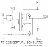
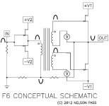
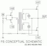
These two conditions must exist for a past published reference like F6:
The first schema shows a special OP-AMP "AP12520", the Tango interstage (driver-) transformer N500-30 (2x 500 ohms to 2x30 ohms) and Toshiba MOSFET 2SK1530
These two conditions must exist for a past published reference like F6:
- The output devices must be connected exactly as shown in the simplified schematic of F6. Thus, the output to the loudspeaker must not be taken from the junction of opposed drains [or bjt collectors], and from the junction of opposed sources [or bjt emitters].
- The gates [or bjt bases] of the semis must be driven in-phase by matched signals from matched secondary windings of the interstage transformer.
1 key issue here: looking at ZM's Post #281 schemo's (easier to look at and see what's there) the bottom fet will have gain, the top FET will have practically none (1). If the XFRM'R is equal secondaries, the bottom FET rules!
N.P. has said there is some very symetrical action going on here? I don't see it, except for the transfomer, and that is not even true because they both are driving a different load???
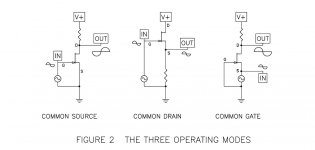
flg. Ignore [Z load] for the time being. For simultaneous positive signals to the gates, the upper fet [is a common drain or voltage follower Vg = 1] drives the lower fet [common source Vg >1]. The impedance of the bottom fet must be much higher than [Z load] to be useful. And it is intrinsically high because one is looking into the drain port [like the collector for bjt]. For simultaneous negative signals, the upper fet [now is a common base; no voltage gain; but has a low input impedance at its source] is the load for the same lower fet working in the common source configuration. For the circuit to be useful, the low impedance of the upper fet's [common base] must be much higher than [Z load]. Otherwise current bypassing/shunting happens. The dynamic impedance of the FETs can't be taken in isolation from [Z load]. Or one must take into consideration the magnitude of the dynamic impedances of the Fets relative to [Z load] to make sense of the circuit.


More like testing our audio knowledge. Was a fun exam!I knew it was a mistake.
Yes, if schema from post #1 would be right. But no after correction - go to post #292.that circ is completely traditional - same sex parts driven with opposite phase signals
while Papa's sketch is showing same sex parts driven with identical ( both in amplitude and phase ) signals
Last edited:
oH....
Now I see what the excitement is about. The leads are reversed on the
original posting. Here is the corrected copy.

Papa , you're Genius ........ with double redish eyes ..........
Attachments


More like testing our audio knowledge. Was a fun exam!
more like mass hysteria ........

this is umpteenth time that Pa pulled my leg up to the sky
call me Naive ZM
- corrected schm after 290 replies- Home
- Amplifiers
- Pass Labs
- F6 Amplifier