The problem with parasitic capacitances is that their effects are frequency dependent. It is very unlikely that picking a point on the MOSFET I-V curve could overcome these asymmetries.1 MOSFET does not output a semetrical sinewave at the input!
2 MOSFETs of the same type "may" have a curve sufficient to find an operating point where, the non lineararities(unsemetrical performance)(distorion) of one, is mirrored by the other, in which case the nonlinearities cancel. But, have you won the lottery lately?
Otherwise, I agree, the Circlotron has the best oportunity to be such a balanced, symetrical, linear design.
I'm not building an F6 after I'm done with my F4 & 5, I'm building a SiClotron
Here is the AC Analysis plotI hate capacitors.
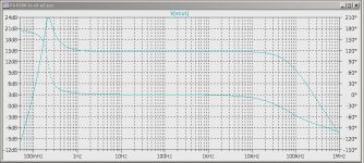
I have been experimenting with "tweaks" in my bias circuit in an attempt to lower THD at low frequencies and discovered that it is possible to provoke oscillation at .2-.3Hz, depending on the RC time constants related to the capacitors. Looking at the LTSpice AC analysis plots, there is a peak in the response at these frequencies and very bad phase margin.
I need to crack open the books and learn how to solve this problem.
Attachments
We have to add some studies on the behavior of the transformers. I had some telex converter coils laying around, and thanks to ZM is tried them.
Two pictures:

Without proper loading
Here we see much ringing.

With proper loading.
With 680 ohm loaded it becomes well behaved. Maybe a little lower would work in my case; my coil has 200 mH inductance.
Loaded this way, the Xfrm (see below) has a bandwidth of 70 Hz- >50 kHz, with a tilt at 200 KHz of about 10 dB.
With feedback it will change it's behavior of course . . .
My work on an "F6":

and
Now testing . . .
This is my prototype board:

Left the bias circuits; center the buffer and feedback stages; right the transformers (1:1), so I use two per channel.
The transformers came from this unit (thanks to ZM!!)

Two pictures:
Without proper loading
Here we see much ringing.
With proper loading.
With 680 ohm loaded it becomes well behaved. Maybe a little lower would work in my case; my coil has 200 mH inductance.
Loaded this way, the Xfrm (see below) has a bandwidth of 70 Hz- >50 kHz, with a tilt at 200 KHz of about 10 dB.
With feedback it will change it's behavior of course . . .
My work on an "F6":
- input with 2SK170/2SJ74
- a bias with the jFET 2SK30AGR/bias resistor of 1k2.
- this works well in principle though the large swing of the output WILL influence the drain current; that is why I have a low pass filter added. The 2SK30 can accept up to 80V loaded this way.
and
- with IRF130 or
- with 2SK1020 (as far as I can see, in specs similar to the R100)
Now testing . . .
This is my prototype board:
Left the bias circuits; center the buffer and feedback stages; right the transformers (1:1), so I use two per channel.
The transformers came from this unit (thanks to ZM!!)
Attachments
Here is the AC Analysis plot
I'm really puzzled- are we going to have that in real life .........
in fact , I'm not puzzled

what's source impedance , when you measure F3 of 70Hz ?
I had the signal generator directly on the coil, <10 ohm I think. No input resistor.
albert
I suspect this is the same as what is called "moter-boating" in tube amplifiers (with transformers). I need to study the solutions used there.I'm really puzzled- are we going to have that in real life .........
in fact , I'm not puzzled
triode_ al: I like [and hopefully others will appreciate] your schematic in post #1023 because:
- The bias to the upper MOSFET is referenced to the output and not to ground. Thus; this MOSFET will always operate Class A. By contrast, lhquam has the corresponding bias in his prototype referenced instead to ground.
- The bias to the upper MOSFET is [hopefully] stable due to the CCS you used to establish it. I would have used [on paper] an independent power supply of positive voltage higher than the rail voltage shown. Bias in this newer instance will be granite solid or better. By comparison, kasey197, uses a resistor voltage divider to establish bias in his prototype. It may suffice. But; it may also appear to be less robust [rock stable] than the one you are using.
- The bias to the bottom MOSFET can be anything else that is stable; which you do show, and others do.
- The blocking capacitors in series with the gates of the MOSFETs eliminate the dreaded direct current through the secondaries.
Last edited:
Perhaps this isn't classical motor-boating after all. The phenomenon occurs when the only caps are the ones in the path from the secondaries to the gates. It looks to me like a LC resonance of the transformer inductance and coupling caps.solution for motor-boating is always easy - brute force - use zillion of uF
it wasn't easy in time when uF was expensive
I found the output offset to be unstable if the upper bias circuit is referenced to the output. When grounded it is stable. Unfortunately, the THD appears to be increased.
triode_al: I like [and hopefully others will appreciate] your schematic in post #1023 because:
- The bias to the upper MOSFET is referenced to the output and not to ground. Thus; this MOSFET will always operate Class A.
- The bias to the upper MOSFET is [hopefully] stable due to the CCS you used to establish it. I would have used [on paper] an independent power supply of positive voltage higher than the rail voltage shown. Bias in this newer instance will be granite solid or better.
- The bias to the bottom MOSFET can be anything else that is stable; which you do show.
- The blocking capacitors in series with the gates of the MOSFETs eliminate the dreaded direct current through the secondaries.
I found the output offset to be unstable if the upper bias circuit is referenced to the output. When grounded it is stable. Unfortunately, the THD appears to be increased.
lhquam. Your bias scheme for the upper JFEt is referenced to ground. This led me to suggest a hypothesis that it may cut off. Does it cut off in your opinion? Interestingly, your prototype works whether this JFET cuts off or not. You may already have a new mode of operation for Conceptual F6!
No, none of the JFETs cut off unless the load is lower than 8 ohms and the output power forces the amplifier into class C.lhquam. Your bias scheme for the upper JFEt is referenced to ground. This led me to suggest a hypothesis that it may cut off. Does it cut off in your opinion? Interestingly, your prototype works whether this JFET cuts off or not. You may already have a new mode of operation for Conceptual F6!
Look at the time constants involved with the gate capacitors and the bias resistance. The time constant is about 1/3 sec. A simple modification to the biasing scheme allows for DC bias to reference to ground while coupling AC from the output, getting the best of both worlds. I was experimenting with that circuit yesterday when I discovered a dangerous low frequency (< 1Hz) oscillation that must be dealt with before going further.
No, none of the JFETs cut off unless the load is lower than 8 ohms and the output power forces the amplifier into class C.
Look at the time constants involved with the gate capacitors and the bias resistance. The time constant is about 1/3 sec. A simple modification to the biasing scheme allows for DC bias to reference to ground while coupling AC from the output, getting the best of both worlds. I was experimenting with that circuit yesterday when I discovered a dangerous low frequency (< 1Hz) oscillation that must be dealt with before going further.
lhquam: Thank you for your response. The bias approach in your prototype of Conceptual F6 is an interesting and unique development.
Everything the Xfrmr "see's" C, R, L and FET Gate's? are all part of it's load. It can be optimized but getting close is ussually easy by the mfg's suggestion or copying a similar configuration. The FET gate will ussually dominate the C parameter you'l find difficult to satisfy in this configuration.

- Home
- Amplifiers
- Pass Labs
- F6 Amplifier