ZM. I agree. The upper JFET will cuttoff after Vo exceeds the fixed dc value of bias if/when referenced to ground .
don't be so sure
")
(it's gate is bootstrapped )
ZM: I often have uncertainty. Pls take a look at post #38 and the schematic therein. The bias scheme for the upper bjt is bootstrapped to Vo, and thus float up and down with it.don't be so sure
(it's gate is bootstrapped )
ihquam. Will it help to see on the scope sine signals in addition to square?
R1*C5 doesn't have any special relation , at least not for me ;
and that scenario of xformer loading was just one of several , which I already mentioned
which one you'll decide to pursue , is up to you
all will lead to same result - proper loading of secondary , proper gate feed , stable bias
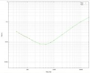
I changed R12 and R13 back to 47K and added 100K pots across the secondaries and adjusted the pots to minimize THD at 40Hz. The minimum occurred at very low values: 409 ohms across the upper fet, and 900 ohms across the lower fet. Is this believable? Here is the resulting THS vs Freq sweep. The loading made only a minor reduction in the THD at low frequencies.
Attachments

lhquam,
i. Re post 984. The loading of the tx secondaries is to flatten the peak we sometimes see at the top end. If your freq response is already flat, then you would not normally need it. Indeed, in the specs for various signal transformers, manufacturers sometimes specify termination resistance and sometimes they do not. The technical paper on Jensens site has a good discussion on this.
ii. Re my questions on gain and feedback. I'm not suggesting that your scheme is incorrect. However, for this topology as Antoinel, NP and a few others have pointed out, it is crucial that the top and bottom fets see the exact same conditions. I found that this was difficult to do easily. In many of the configs I tried, I ended up with the top and bottom halves contributing differing gain amounts. The effect was only visible open loop with any potential local fb loops eliminated (ie transformer is bypassed for the 'dead' fet + battery bias for the same, no global fb) Tedious - agreed but it seems really worthwhile to nail this correctly lest we end up with a transformer input JLH in disguise. When I gave the [edit:] gate of top fet any lowish resistance return to ground, its gain changed, indicating a local fb loop. In your example, reducing R12 & R13 increased local fb & caused reduced thd. Overall gain might not change much though - as we all know that's one of the key 'contributions' of nfb - to dampen the effect of gain variations in the amplifying blocks towards the systems total gain.
iii) In the event that this line of thinking interests you, might I offer two suggestions ?
a) You can minimise the local fb (if that is your desire) by increasing the resistance in the biasing network (see F1 service manual http://www.firstwatt.com/pdf/prod_f1_srv.pdf for an example). It might be the case that the resistors are already high enough in value and therefore all is well but worth noting that NP used 27k with the R100s but it had to go as high as 0.5M with the IRF parts ! I don't know if 27k is [edit:] high enough (with gate stoppers at 22R) but there's only one way to find out for sure.
b) Whatever biasing network etc you end up with, its worth measuring the top and bottom halves gain as described in (ii) above to ensure that you're getting what you expect. If the two gains are materially different: rinse, wash & repeat
Interesting thread .....
Last edited:
I'm not convinced there is voltage gain from the top FET? The input is G-S, the output is the Source. It's Common Drain/Source follower
my vote is for
Would that put your calculation results where you think they should be?
flg, I, like you, took a while to be convinced, but did some thinking and agreed that it did in fact provide current/voltage gain in common source mode. Simple experiments as posted on #561 in this thread showed that was the case as well.
kasey197: Your schematic in post #161 shows that the bias for the upper JFET is referenced to the output node. It rides up and down with the output signal Vo. The upper JFET is always in Class A.
ihquam: Your schematic in post #941 shows that the bias for the upper JFET is referenced to ground instead. The gate-source junction of the upper JFET will reverse bias as Vo goes positive relative to ground. The upper JFET can cut-off and switch to Class B
The two biasing schemes above are different with different operational outcomes: I am not sure whether my read is correct. But; which of the two biasing schemes do you think is in the actual design of Mr. Pass? I have a preference to that of kasey197.
Member
Joined 2009
Paid Member
sorry in advance for a dumb question !
I remember reading Nelson's article on negative feedback, it left a lasting impression on me. There are many benefits to avoiding negative feedback. And when a transformer is in the loop it adds it's own challenges. So if this circuit has -ve feedback I am curious as to why ?
I remember reading Nelson's article on negative feedback, it left a lasting impression on me. There are many benefits to avoiding negative feedback. And when a transformer is in the loop it adds it's own challenges. So if this circuit has -ve feedback I am curious as to why ?
kasey197: Your schematic in post #161 shows that the bias for the upper JFET is referenced to the output node. It rides up and down with the output signal Vo. The upper JFET is always in Class A.
which of the two biasing schemes do you think is in the actual design of Mr. Pass?
>>Naw I dont find that. Vgs for upper fet = variable signal voltage across tx sec + fixed vgs bias voltage. Second term is only 1.x V. Upper fet switches off ultimately and we move into class B. Experimentally, for the R100s and using the biasing scheme mentioned above, I see clipping (by that I mean 1% thd) at 44V RMS across at 6.8R load = 140Wrms with +/-24 V rails. Thats way beyond what the 1.6A bias can support into class A.
>>Dunno and I think either works ok provided we dimension the resistances accordingly. Which one he chooses will depend as always on the magic of the operating points chosen which we cannot guess. There are somethings though that we CAN guess with some amount of certainty:
a) PASS = Performance Amplification through Sophisticated Simplicity {Da Vinci said that simplicity is the ultimate sophistication ...}
b) If some funky fb trick is used (see Watts New update from long ago0, then perhaps we'll see high-z bias network to reduce/eliminate local fb and caps in series with the tx primary.
c) If fb is as is shown on the conceptual schema and tx is set for 1:1, then I'd guess low-z bias network with local and global fb. This is the scheme he used in ZV5.
I guess we can play with some of these variations ourselves. I can follow a recipe fairly closely but can never replicate a dish exactly. If we have just an idea of some of the ingredients, our results will unlikely even be close
Last edited:
I just know that in the end, it will be some sematic resolution that really isn't worth arguing over, I will be the loser, etc, etc.flg, I, like you, took a while to be convinced, but did some thinking and agreed that it did in fact provide current/voltage gain in common source mode. Simple experiments as posted on #561 in this thread showed that was the case as well.
So, I went off and powered up the PSpice. How pany posts in this thread are about the (Corrected) Simplified F6 Schemo? And how many about a working pile of semi cunducting mess? I've heard everything, at least that I wanna read. This wasn't a post about mess's
Now I'll go find 561?
So, the 1st issue is, Avol contribution of the top FET. The Consencus seems to be, it has equal AC voltage gain contribution as the bottom FET
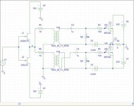
In the Simplified Sim Model I put together, pictured below, I think I capture the important funtions??? Fed with .1V 1kHz Most of the circuit is totally obvious, including "simplified" area's. Out of the top Transformer winding comes 5.8VAC + or -. But thats not the transformer output, it's a 1:1, that's the bias plus the transformer Sec output, plus the voltage variation at the drain of the bottom FET. So in order to see the actual Gate to source we need a diff probe not refrenced to gnd but to the Vout node (FET Source). Walla!, now we see .1V on the gate of the MOSFET refrenced to the Source of the MOSFET
And, what you've all been waiting for... ... ... Yea, the output node of the top FET is the source, and on the source is the Drain variation of the bottom FET plus .1V (+ or -). No Gain fromk the top FET.
The Bottom FET appears to have a voltage gain of about 58. Strange these numbers seem familiar?
Attachments
Interesting. To check your results, why dont you just measure the voltage across the load R7 and alternately remove C4 and C5 (ie leave them open circuit in turn). Based on your post, you should see 5.8V with C5 open and C4 in place. And 0.1V with C5 in place and C4 open.... is that the case?
hi all,
Had time...
Results:
0.2V pk-pk in, 9.8V pk-pk out. Therefore gain = 49x. Given the tx gives us 4x, that means the fets are giving us approx 12.2X gain.
Theory:
Load R = 6.8R, therefore combined bottom n top half transconductance = 12.2/6.8 = 1.8 Siemens. Each fet therefore gives us 1.8/2 = 0.9 S transconductance. This seems to tie in with what i see from the hitachi datasheets.
Explanation:
Given the above, both top and bottom fets are acting in common source mode (despite the temptation to think about the top half as a source follower providing no voltage gain). If this hypthesis is true then both top and bottom halves provide equal amounts of gain. We can test this easily given the transformer coupling by just bypassing the top and bottom tx secondaries (ie in turn, each fet would see only the bias voltage, but no signal) individually and seeing the effect.
Results:
Both secondaries connected, trace 1. Output is 9.8V.
Top secondary bypassed, trace 2,. Output is 4.875V
Bottom secondary bypassed, trace 3. Output is 4.812V
Summary: So, the sum of the two halves individually = 9.7V vs 9.8V when theyre both connected. Seems close enough to suggest that the initial hypothesis that both halves act to provide equal amounts of gain (in common source) is correct.
Wow? Lets see what the flg prototype in Pspice does? I had to think more to take out the top Xfrmr so rather than do that, I took the easy way out, I put a big resistor in series with the xfrmr...
As pictured in the previous post, I actually get 5.78Vout with .1V in. These are all Peak AC Volts. ie: .0707Vrms input.
With a 30Mohm resistor in series with the top transmormer instead of the Cap, essentially creating a huge voltage divider to the ac signal, the Vout is 5.822V. That appears to be less than 1% gain change w vs w/o the top Secondary winding

Some other results/thoughts:???
So, I went a little further and found that using 30M in my sim didn't make the same results as 30000000 when descibing a resistor value. I also found some strange results? For instance, now when I insert a 30Mohm resistor in the top or the bottom xfrmr I get about 1.7Vout? Gain of 17?
I need to work out a few more things to get this strait myself now
I need to work out a few more things to get this strait myself now
I am working on the biasing issue at this moment. I first connected the bottom of the biasing network to the output, but found that the output offset voltage would not stabilize, since there is no DC negative feedback in this amplifier. I connected it to ground and achieved solid output offset stability at the cost of increased THD.
Today I made circuit changes that provide both DC stability and AC coupling of the output to the upper bias network. I am running tests now and will post results.
Today I made circuit changes that provide both DC stability and AC coupling of the output to the upper bias network. I am running tests now and will post results.
kasey197: Your schematic in post #161 shows that the bias for the upper JFET is referenced to the output node. It rides up and down with the output signal Vo. The upper JFET is always in Class A.
ihquam: Your schematic in post #941 shows that the bias for the upper JFET is referenced to ground instead. The gate-source junction of the upper JFET will reverse bias as Vo goes positive relative to ground. The upper JFET can cut-off and switch to Class B
The two biasing schemes above are different with different operational outcomes: I am not sure whether my read is correct. But; which of the two biasing schemes do you think is in the actual design of Mr. Pass? I have a preference to that of kasey197.
sorry in advance for a dumb question !
I remember reading Nelson's article on negative feedback, it left a lasting impression on me. There are many benefits to avoiding negative feedback. And when a transformer is in the loop it adds it's own challenges. So if this circuit has -ve feedback I am curious as to why ?
i also found that an excellent article. The need for nfb is also covered in the same piece but here, for such an intrinsically linear amp, i would think that the primary need for nfb is to reduce the output impedance so that we can get closer to voltage source amp i/o a transconductance or current source amp.
it's easy to determine gain contribution of upper Jfet - either Spice or measure on real circ:
measure output voltage as is , and with upper Jfet without modulation (disconnected secondary of xformer)
I'm too lazy to make graphical files for analogy of OS with plain resistors
measure output voltage as is , and with upper Jfet without modulation (disconnected secondary of xformer)
I'm too lazy to make graphical files for analogy of OS with plain resistors
i also found that an excellent article. The need for nfb is also covered in the same piece but here, for such an intrinsically linear amp, i would think that the primary need for nfb is to reduce the output impedance so that we can get closer to voltage source amp i/o a transconductance or current source amp.
The nice thing with this circuit is that the feedback has no influence on the input circuit itself.
So I plan to go for closed of loop 30 dB, not 15 dB, and see for myself. R1=10Ω, R2=300 or 330 Ω.
- Home
- Amplifiers
- Pass Labs
- F6 Amplifier