thanks again for fb
I measure the bias with DVM set to V and Vgs reads about 1.15 to 1.2 V and are set together with the bias pot.
the DC offset is measured at the output and goes from -13V to -11V (not millivolts but Volts) with offset pot. This is my main concern at this point.
The other channel DC ofssets correctly and is set to 0mV
say that you want 1A6 through outputs
that means - one DVM across one of 0R1 source resistors (or one 0R1 temporary placed series in one rail , if you're not using source resistors) , other DVM between output and GND
for 1A6 Iq , goal is to gave U=IxR=1A6x0R1=0V16 across mentioned source resistor ......... and 0V at output
as others already said - fiddle with pots one by one , in same increments
if you can't achieve either current or offset - increase reference voltage - more LEDs or LED with greater Usat
green is in range of 1V93 , so .......

Ok ,
lets call an apple an apple,
I'm measuring Vgs and they measure between 1.153 and 1.2V
The dc offset at output are at 0V on one channel and cant get past -11V (-11000 mV) on the other channel.
Both channels are identical. At this point, I don't think the problem is adding more leds. I trierd an extra led on the problem channel with same result. It seems that it is something else causing this issue.
Measuring Vgs is a misnomer. It assumes that you have perfectly matched pairs at the exact temperature they are operating at. Are you using source resistors? Your fet is not burnt up or you would see ful rail voltage on output. You have one fet that is turned on more than the other. From the looks of it, it is the upper fet of channel 2. Try reducing the bias on the upper fet and see what happens to the offset.
measurements with outputs removed from circuit
always getting 0v at .1r source resistor
always getting 2.6mV at output
this is regardless of pot settings.
Turning bias pot and setting Vgs at 1.2V at Q2 no movement of Vgs at Q1
turning offest pot and moving Vgs at Q1 to 1.2V
still getting 0v at .1r source resistor
2.6mV at output
always getting 0v at .1r source resistor
always getting 2.6mV at output
this is regardless of pot settings.
Turning bias pot and setting Vgs at 1.2V at Q2 no movement of Vgs at Q1
turning offest pot and moving Vgs at Q1 to 1.2V
still getting 0v at .1r source resistor
2.6mV at output
dunno how I can explain better
with outputs out of circuit :
turn P1 all the way CCW and write what voltage you have between R7 (irrelevant which leg) and gnd ;
turn P1 all the way CW and write what voltage you have between R7 (irrelevant which leg) and gnd ;
turn P2 all the way CCW and write what voltage you have between R8 (irrelevant which leg) and neg rail;
turn P2 all the way CW and write what voltage you have between R8 (irrelevant which leg) and neg rail;
take few proper resolution pictures and post them here
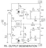
all that referring to this schematic :
with outputs out of circuit :
turn P1 all the way CCW and write what voltage you have between R7 (irrelevant which leg) and gnd ;
turn P1 all the way CW and write what voltage you have between R7 (irrelevant which leg) and gnd ;
turn P2 all the way CCW and write what voltage you have between R8 (irrelevant which leg) and neg rail;
turn P2 all the way CW and write what voltage you have between R8 (irrelevant which leg) and neg rail;
take few proper resolution pictures and post them here
all that referring to this schematic :
Attachments
Last edited:
turn P1 all the way CCW and write what voltage you have between R7 (irrelevant which leg) and gnd : 1.825V
turn P1 all the way CW and write what voltage you have between R7 (irrelevant which leg) and gnd 0V
turn P2 all the way CCW and write what voltage you have between R8 (irrelevant which leg) and neg rail; 1.825V
turn P2 all the way CW and write what voltage you have between R8 (irrelevant which leg) and neg rail 0V
now
-turn both pots all the way CW (case with min. voltage corresponding to #5614)
-mount outputs back , confirm proper isolation from heatsink
-put one DVM between output and gnd
-put one DVM across R14 (ref to sch in #5613)
-power up
**-turn P1 for one full turn, then turn P2 for one full turn
-observe what's happening
repeat exactly step marked with ** as long you start to see something changing at DVMs ..... then proceed in half-turn steps
catch is in iterative setting of two pots - lower one is setting current (say that you want 1A5) while upper one is setting 0 at output (which is exactly what you want - everything up to 50mV is normal)
during that procedure - ignore and do not measure what's Ugs voltage - it is irrelevant and not likely be ever identical for lower and upper output!
if you arrive at full CCW position of both pots without having desired Iq (voltage at R14 - for 1A5 Iq needs to be 0V15) , change LEDs for some with higher voltage , or put another LED in string ( in both positions)
green LED is in range of 2V , while blue one is slightly above 3V , at least those I have
fine set everything ( fiddle with two pots ) when amp is in temp. equilibrium
Last edited:
is this normal when the semis are soldered back in:
turn P1 all the way CCW and write what voltage you have between R7 (irrelevant which leg) and gnd : 1.625V
turn P1 all the way CW and write what voltage you have between R7 (irrelevant which leg) and gnd 0V
turn P2 all the way CCW and write what voltage you have between R8 (irrelevant which leg) and neg rail; .225V
turn P2 all the way CW and write what voltage you have between R8 (irrelevant which leg) and neg rail 0V
is this normal when the semis are soldered back in:
.....
turn P2 all the way CCW and write what voltage you have between R8 (irrelevant which leg) and neg rail; .225V
.....
no that i snot normal
same as it is not normal to do what no one tell you to do - to fiddle with pots to max , while having outputs in place
now you need to test them - out of circuit or in , your choice
or just go and buy new pair of SSouths
I gave you exact recipe what to do , everything you made now is for your own disaster
Its is very possible that when you were biasing the output originally, you were paying attention to Vgs of the fets and not Iq of the output. If you had fets with low Vgs for a given I, then you could have fried it while trying to align the Vgs.
When biasing an output stage, the only thing that matters is Iq and offset, nothing else.
When biasing an output stage, the only thing that matters is Iq and offset, nothing else.
- Home
- Amplifiers
- Pass Labs
- F6 Amplifier