tnx Buzz
hopefully , I'll not forget it this time
let me know when you , whenever , try 6-fillar
damn ..... I just remember that I have somewhere some nice toroid nickelsomethingamorphous cores ........ gonnna threw them to winder guy ......
damndamn - I just realize , again , that I simply have no use even for smallest balanced F6 like amp ........
Next thing i will be trying is M2 look a like. After that, picking up again SE fed(or balanced), bridged SiT for a friend using 5 filar.
.........
I have quickly wired F6 up......
just go for it
Next thing i will be trying is M2 look a like. After that, picking up again SE fed(or balanced), bridged SiT for a friend using 5 filar.
naah ....... M2 is amp for sissies ..........
(like ZM , for instance .........
 )
)btw - you really need to try all these 15" you have , cobbled together on bigbadaz OB

Attachments
Last edited:
not yet , and most probably will not
too lazy ....... or they're too perfect as is -blessed by position .... mimicking U-frame
Enjoy

Transformer Super Guru is who you are for writing Babelfish F6...schematic.I know that ...... made xformer microphone stereo matrix maybe even before I knew how to solder properly (well , with my Guru above my head , using Bolex telescope as teaching device
but , where's the challenge then ....... certainly not mixed with simplicity
Hi Semisouthfan,
Thank you for sharing your knowledge on Sic Jfet. Also, you are right I was meaning 'winding resistance' when I was saying 'transformer impedance'.
I have quickly wired F6 up with lundahl LL1690 which has 150ohm resistance in each windings. It takes about 1.5v Vgs for 1.5A bias and is stable so far for a couple of hours now. Does it mean those Jfets have acceptable gate leakage current? Or does it take a while before I can be sure?
Thank you.
Hey, if it works, don't fix it!
The only issues I have encountered are at DC, where in some circuits (for
reasons of simplicity) you wish to bias the Jfet through a high value resistor
so as to have a high input impedance. In that case, Gate leakage becomes
part of the DC equation, and is typically a factor above 10 Kohm so so.
Transformers actually alleviate this, as their DC impedance is usually 100
ohms or less, but their AC impedance can be high.
In either case, it takes pathologically high leakage figures to create
problems for these audio circuits, and I cull any such cases out in testing
as being defective parts.
I agree with Nelson but I would like to make a distinction that might not have been clear in my first post on the subject. There are two possible sources of gate leakage: Reverse bias gate leakage and forward bias gate leakage. Both are "normal" provided they are within data sheet limits (and then some). They should be observed and treated independently of each other. For an enhancement-mode SemiSouth SiC JFET (think R100, R100A, or R125), when the transistor is biased Class A the gate leakage current should be dominated by the forward bias current of the SiC gate-source pn diode. If it is, then the normal gate bias resistances (kiloohms up to maybe a few 10's of kiloohms) will be no issue.
Checking a gate-source diode to see if it is too leaky, as opposed to just the normal amount of leakiness, should be done by reverse biasing the gate with respect to the source. I check all of my parts for this as a matter of course. The data sheet specifies no more than 300 microamps at VGS = -15 V (that current at VGS = -10 V for the R100A), but in practice much larger than this (two or three times) will not really effect the circuit, especially when you consider that in the amplifier you are putting +1.5 volts on the gate NOT -15 V!! For most parts that seem leaky at -15 V, or even -10 V where the R100A is specified, will usually have negligible leakage current at VGS = -1.5 V. In that case, the leakage current at VGS = +1.5 V is virtually always the "normal" amount for the forward bias applied. (Naturally, if you are the somewhat less common SemiSouth Fan and you like depletion mode parts, then reverse gate leakage is an issue for you, but SemiSouth had fewer problems with leaky gate-source diodes with the depletion mode variety.)
Only an extremely (pathologically?) leaky gate will effect the biasing of the transistor above threshold. I call that kind of gate leakage "anomalous." SemiSouth knew that parts with anomalous gate leakage had manufacturing defects in the gate-source diodes and did not knowingly release them into the general population. In contrast, the SJEP120R100A was marketed specifically for non-switching applications (i.e., audio) because the higher gate leakage of these parts at VGS = -15 V had no effect at all on Class A amplifier operation. You can't tell the difference between R100 and R100A operation due to gate source leakage. Unfortunately, the question has become a source of worry for DIYAudio folks when it should not be.
When I come across parts with anomalous gate leakage I don't supply them to others. But I do set those that still test good for low gate-drain diode leakage aside for future use. These parts are great for fooling around in the lab with experimental amplifiers because in Class A they still work great, even with milliamps of gate leakage!!!
The correlation between gate leakage and DC bias instability is, in my experience, mostly a matter of thermal runaway. As the junction temperature goes up, so does the forward gate leakage, which can load down the gate bias resistors. Positive equivalent series gate resistance will ballast this somewhat, but too much gate resistance will cause the JFET operating point to end up where you don't want it. This is totally normal and pursuant to the laws of physics in good parts. That is why the equivalent series gate resistance while biasing the enhancement-mode JFET is recommended to be less as compared to the MOSFET. It's simply the rules of the road. Therefore, biasing the critters too far above threshold may require a more proactive effort to ensure bias stability (i.e, more feedback). Fortunately, the preferred operating points for the F6 that I have been told about don't push the JFET with the normal threshold voltage range into this coffin's corner.
Surprisingly, anomalous gate leakage is usually more resistive than diode-like so there is often not the same strong temperature dependence that you expect from the normal pn diode. That's why the parts that I set aside with "blown" gates still can work great in a Class A amplifier. I'm a pack rat and kinda cheap, so reusing such castoffs makes me feel, well, happy. Cheap, but happy.
whenever you are ready , I'll be more than happy to take care of these leftovers , in OPLDF ; shipping , as usual , on your charge
Get the hint? Semisouthfan = Cheap.
Get the hint? Semisouthfan = Cheap.
I would call it being resourceful. The best engineers I've known and worked with are all the same. Part of being a good engineer is making good use of the available resources. Creating solutions that are simple and less costly. Sometimes that means saving things you currently have no use for.
I would call it being resourceful. The best engineers I've known and worked with are all the same. Part of being a good engineer is making good use of the available resources. Creating solutions that are simple and less costly. Sometimes that means saving things you currently have no use for.
Not to mention it can be just cool to pull junk out of the box and turn it into music!
Hi,
Problem.
After playing music for several hours suddenly one channel distorted and showed about 500mv of DC offset. One of the Jfets was almost turned off, and the other one was conducting more than initial bias current. Heat sink fins were about 55 C according to the "skin test". Amp works normally again after cooling it down and the problem has not shown up again yet.
Since I am not using the same components as in original F6 I have some concerns.
1. transformer with higher winding resistance(150ohm).
2. single-end buffer(2x2ks170BL like in B1) that might have higher output impedance than push-pull buffer in original F6.
Do you think this problem might be related to the gate leakage issue?
Or is it 'Thermal runaway' that Semishouthfan mentioned in previous post?
Thank you.
By the way, this Amp sounds too good to give up!
This is my second Firstwatt clone project. I thought the first one(BA3+F4) sounded really good but when I listened to F6 I liked it more by a big margin.
trivial question - are (all) Jfets properly thermally connected to heatsink?
try ferrite beads instead of gate resistors , to compensate for increased winding resistance
Yes, they are bolted to heatsink with mica and greese.
Jfet pins are not soldered yet. I am using molex sockets temporarily.
You mean, R5 or R7?
I wrote - gate resistors (of output Jfets )
show me schematic you're using and I'll say which ones
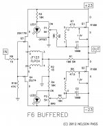
I attatched the schematic I used.
Attachments
- Home
- Amplifiers
- Pass Labs
- F6 Amplifier