HI ALL
voltages are 1.3v at p1 one and .1mv at p2
here are some pics
the zeners are being used as I stuffed the led,s taking them out to check if they were ok
this channel is built exactly the same as the working one ive double checked and its got me stuffed
voltages are 1.3v at p1 one and .1mv at p2
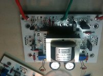
here are some pics
the zeners are being used as I stuffed the led,s taking them out to check if they were ok
this channel is built exactly the same as the working one ive double checked and its got me stuffed
Attachments
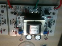
Same colour wire for V+ and V- is trouble on the right hand photo.fet hole next to p2 says -27.5v
fet hole next to p1 says 171mv
Measure across first hole(gate pin) and third hole(source pin) where the fets will go. Also, on P1 side, measure from ground to top of Led. This would be the right side of the 10K resistor directly above it. On the P2 side, measure from negative rail to top of Led. THis would be left side of 10K resistor directly above it.
worked it out
the daughter board on the faulty channel is around the wrong way ,the worst part is I soldered it in as I never planed on messing with transformers !!!!!
now I have to get the bloody thing off some how
I can see many hours with solder wick in my hands
Sheafer
the daughter board on the faulty channel is around the wrong way ,the worst part is I soldered it in as I never planed on messing with transformers !!!!!
now I have to get the bloody thing off some how
I can see many hours with solder wick in my hands
Sheafer


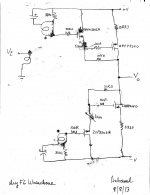
The interface to the transformer's secondaries was blurry and unclear in the above post. The top part of the attached picture shows 2 options. The right option is the one which was blurred; e.g. for the P channel L'Fake SIT. I figured the 33K2 resistor in wrenchone's parent schematic introduced a needed [sizeable] impedance to the input signal. The top left scheme is simple and may not need the 33K2 altogether to generate the current source which is modulated by the input signal.
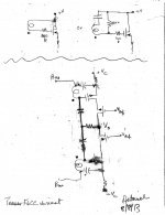
The bottom portion of the attached picture is a simplified variant of lhquam's Teaser F6cc. The Schade/Pass feedback schemes in wrenchone's methodology above are equally adaptable in this case. The added [emphasized] components are 2 DC blocking caps and one feedback resistor. This arrangement is expected to convert the amp's original pentodish characteristics to the desired triodish characteristics via this SIT faking process.
The bottom portion of the attached picture is a simplified variant of lhquam's Teaser F6cc. The Schade/Pass feedback schemes in wrenchone's methodology above are equally adaptable in this case. The added [emphasized] components are 2 DC blocking caps and one feedback resistor. This arrangement is expected to convert the amp's original pentodish characteristics to the desired triodish characteristics via this SIT faking process.
Attachments
- Home
- Amplifiers
- Pass Labs
- F6 Amplifier