I present the Balanced F5 in a Small Footprint.
I have finally completed testing of my balanced F5 PCB which is optimized for use with a relatively small 5" x 7" heatsink. This effort with inspired by EUVL's F5X project http://www.diyaudio.com/forums/pass-labs/121228-f5-power-amplifier-119.html#post1538826 http://www.diyaudio.com/forums/pass-labs/183362-f5x-euvl-approach.html?highlight=f5x, by my previous experience with the Cviller F5 V1.2 boards on a 5" x 7" heat tunnel: http://www.diyaudio.com/forums/pass-labs/206756-f5-turbo-circuit-boards-83.html#post2928566 and by my experience using a heat tunnel http://www.diyaudio.com/forums/pass-labs/121228-f5-power-amplifier-1021.html#post2453420.
I envision five different configurations for using this PCB:
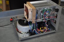
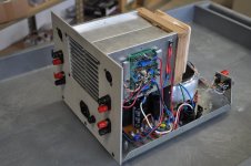
A. Heat tunnel, stereo balanced F5, 17 volt rails, 40-50 W/ch class A. Shown in image below.
B. Heat tunnel, four F5s, 24 volt rails, 25 watts/ch class A.
C. Heat tunnel, stereo F5 Turbo V1, 32 volt rails, 40-50 W/ch class A. PCB partially populated.
D. Heat tunnel, 1 channel balanced F5, 32 volt rails, 100 watts class A, 200(?) watts class AB. PCB partially populated.
E. Small heatsink, headphone amplifier, two F5s, ?? volt rails, ?? watts/ch class A.
I am primarily interested in the stereo balanced F5 configuration A and will concentrate on it in this thread. I couldn't decide what MOSFETs to use for the balanced amplifier of configuration A, so I populated one PCB using FQA28N15/FQA36P15 MOSFETs and another using FQP19N20C/FQP12P20 MOSFETs. All of these MOSFETs are still available from DigiKey and Mouser. I intend to test another board using Toshiba 2SK1530/2SJ201 MOSFETs which are made of virtual unobtainium.
Following posts will show PCB design, packaging and performance results for two configurations:
. FQA28N15/FQA36P15 MOSFETs with Caddock source and feedback resistors mounted to the heatsink.
. FQP19N20C/FQP12P20 MOSFETs clamped to the heatsink and onboard wirewound source and feedback resistors.
I have finally completed testing of my balanced F5 PCB which is optimized for use with a relatively small 5" x 7" heatsink. This effort with inspired by EUVL's F5X project http://www.diyaudio.com/forums/pass-labs/121228-f5-power-amplifier-119.html#post1538826 http://www.diyaudio.com/forums/pass-labs/183362-f5x-euvl-approach.html?highlight=f5x, by my previous experience with the Cviller F5 V1.2 boards on a 5" x 7" heat tunnel: http://www.diyaudio.com/forums/pass-labs/206756-f5-turbo-circuit-boards-83.html#post2928566 and by my experience using a heat tunnel http://www.diyaudio.com/forums/pass-labs/121228-f5-power-amplifier-1021.html#post2453420.
I envision five different configurations for using this PCB:
A. Heat tunnel, stereo balanced F5, 17 volt rails, 40-50 W/ch class A. Shown in image below.
B. Heat tunnel, four F5s, 24 volt rails, 25 watts/ch class A.
C. Heat tunnel, stereo F5 Turbo V1, 32 volt rails, 40-50 W/ch class A. PCB partially populated.
D. Heat tunnel, 1 channel balanced F5, 32 volt rails, 100 watts class A, 200(?) watts class AB. PCB partially populated.
E. Small heatsink, headphone amplifier, two F5s, ?? volt rails, ?? watts/ch class A.
I am primarily interested in the stereo balanced F5 configuration A and will concentrate on it in this thread. I couldn't decide what MOSFETs to use for the balanced amplifier of configuration A, so I populated one PCB using FQA28N15/FQA36P15 MOSFETs and another using FQP19N20C/FQP12P20 MOSFETs. All of these MOSFETs are still available from DigiKey and Mouser. I intend to test another board using Toshiba 2SK1530/2SJ201 MOSFETs which are made of virtual unobtainium.
Following posts will show PCB design, packaging and performance results for two configurations:
. FQA28N15/FQA36P15 MOSFETs with Caddock source and feedback resistors mounted to the heatsink.
. FQP19N20C/FQP12P20 MOSFETs clamped to the heatsink and onboard wirewound source and feedback resistors.
Attachments
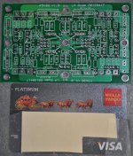
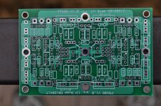
PCB V1.0
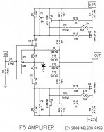
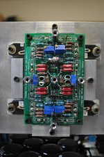
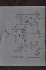
The V1.0 PCB contains two F5 amplifiers with the circuit topology shown here and on page 2 of Nelson's F5 Turbo article http://www.firstwatt.com/pdf/art_f5_turbo.pdf. Version V1.0 was designed and fabricated using ExpressPCB ExpressPCB - Free PCB layout software - Low cost circuit boards - Top quality PCB manufacturing 2.5" x 3.8" 2-layer MiniBoards.
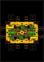
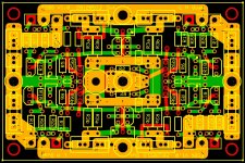
The 2nd image shows the PCB design with outboard MOSFETS and source and feedback resistors in relation to the heatsink (the surrounding yellow rectangle), with the airflow from bottom-to-top. The MOSFET placement was carefully chosen for heat distribution. The design is for 100-120 watts dissipation per heatsink. I borrow heavily from EUVL's elegant PCB layout and its use of standoffs for power and output connections. Two 2-pin headers provide input connections. Two 6-pin headers provide "diagnostic" connections for bias adjustment.
Version V1.0 of the PCB can be used to implement an F5X channel, a balanced F5 channel, or two independent F5 channels. There are 2 major, permanent jumpers for the X connections. Without any other jumpers, the board provides an F5X. Two jumpers provide a floating balanced togolopy, (the X's are connected). Two more jumpers activate Nelson's P3 adjustment. And finally, two more jumpers ground everything for initial adjustment or for use as 2 independent unbalanced F5 amplifiers. Originally, the jumpers were intended to be made using .1 inch shunts, but I abandoned that approach because of lack of good contact pressure and uncertainty about the the contact resistance of the shunts.
The V1.0 PCB contains two F5 amplifiers with the circuit topology shown here and on page 2 of Nelson's F5 Turbo article http://www.firstwatt.com/pdf/art_f5_turbo.pdf. Version V1.0 was designed and fabricated using ExpressPCB ExpressPCB - Free PCB layout software - Low cost circuit boards - Top quality PCB manufacturing 2.5" x 3.8" 2-layer MiniBoards.
The 2nd image shows the PCB design with outboard MOSFETS and source and feedback resistors in relation to the heatsink (the surrounding yellow rectangle), with the airflow from bottom-to-top. The MOSFET placement was carefully chosen for heat distribution. The design is for 100-120 watts dissipation per heatsink. I borrow heavily from EUVL's elegant PCB layout and its use of standoffs for power and output connections. Two 2-pin headers provide input connections. Two 6-pin headers provide "diagnostic" connections for bias adjustment.
Version V1.0 of the PCB can be used to implement an F5X channel, a balanced F5 channel, or two independent F5 channels. There are 2 major, permanent jumpers for the X connections. Without any other jumpers, the board provides an F5X. Two jumpers provide a floating balanced togolopy, (the X's are connected). Two more jumpers activate Nelson's P3 adjustment. And finally, two more jumpers ground everything for initial adjustment or for use as 2 independent unbalanced F5 amplifiers. Originally, the jumpers were intended to be made using .1 inch shunts, but I abandoned that approach because of lack of good contact pressure and uncertainty about the the contact resistance of the shunts.
Attachments
PCB with FQA28N15/FQA36P15 MOSFETS
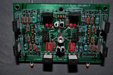
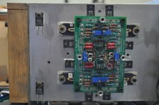
The first PCB was built using FQA28N15/FQA36P15 MOSFETs, .25 ohm Caddock source resistors, and 50 ohm Caddock feedback resistors as shown in the first image. Because of the limited power dissipation requirements, I mounted the Caddocks vertical to the PCB. I later found that this is a bad idea because the leads on the Caddocks are fragile and break after a few flexes. I "repaired" the Caddocks and mounted them to the heatsink using clamps as shown in the 2nd and 3rd images.
The first PCB was built using FQA28N15/FQA36P15 MOSFETs, .25 ohm Caddock source resistors, and 50 ohm Caddock feedback resistors as shown in the first image. Because of the limited power dissipation requirements, I mounted the Caddocks vertical to the PCB. I later found that this is a bad idea because the leads on the Caddocks are fragile and break after a few flexes. I "repaired" the Caddocks and mounted them to the heatsink using clamps as shown in the 2nd and 3rd images.
Attachments
PCB with FQP19N20C/FQP12P20 MOSFETs
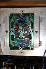
The second PCB was populated with FQP19N20C/FQP12P20 MOSFETs, mounted using clamps, and .25 ohm wirewound source and 50 ohm wirewound feedback resistors. Caddocks could have been used, but I wanted to test this alternate resistor configuration.
The second PCB was populated with FQP19N20C/FQP12P20 MOSFETs, mounted using clamps, and .25 ohm wirewound source and 50 ohm wirewound feedback resistors. Caddocks could have been used, but I wanted to test this alternate resistor configuration.
Attachments
Bias adjustment
To simplify the adjustment of bias current and output offset current, I have provided two 6-pin headers
on the PCB for attaching a "diagnostic cable". This cable is wired to a 6-position, 2-pole rotary switch, connected to binding posts for a multimeter. The rotary switch positions select the following:
1. Vs1+ voltage across P-channel source resistor of amplifier 1
2. Vs1- voltage across N-channel source resistor of amplifier 1
3. Out1 output voltage of amplifier 1
4. Out2 output voltage of amplifier 2
5. Vs2+ voltage across P-channel source resistor of amplifier 2
6. Vs2- voltage across N-channel source resistor of amplifier 2
Attachments
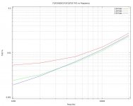
Distortion Measurements
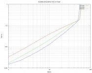
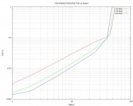
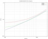
THD measurements were made using SillanumSoft Visual Analyzer 2011 XE Visual Analyser 2011 XE
and an M-Audio Audiophile 192 sound card. The amplifiers were measured in grounded balanced mode with an 8 ohm resistive load. Four sets of graphs, each containing curves at 1.0A, 1.5A, and 2.0A bias currentsare shown:
1. FQA28N15/FQA36P15 THD vs Power at 1 kHz.
2. FQP19N20C/FQP12P20 THD vs Power at 1 kHz.
3. FQA28N15/FQA36P15 THD vs Frequency at 2 watts output.
4. FQP19N20C/FQP12P20 THD vs Frequency at 2 watts output.
At low power levels, the FQP19N20C/FQP12P20 MOSFETs provide lower THD levels than the FQA28N15/FQA36P15 MOSFETs. At power levels above 40 watts amplifier clips, primarily due to the lower transconductance of these MOSFETs. At 40 watts, the THD is similar to that of the F5 Turbo at 40 watts, but much better at low power levels.
With the FQA28N15/FQA36P15 MOSFETs the amplifier produces 50-55 watts with THD around .2%.
This is somewhat higher than Nelson shows for the F5 Turbo, probably due to lower MOSFET transconductance.
Conclusion:
For maximum power, my choice is the FQA28N15/FQA36P15 MOSFETs at around 1.5A bias.
For lowest THD at 1-2 watts, my choice is the FQP19N20C/FQP12P20 MOSFETs at around 2.0A bias.
Attachments
Power Supply
An Antek AN-5415 toroid transformer with four 15 volt secondary windings, is used to power two +16V and two -16V supplies. Each supply uses 1/2 of a 35A 200V Vishay diode bridge, four .022 Farad 35 volt electrolytic capacitors, and a .5 ohm Caddock resistor, forming a CRC filter.
With the diode and CRC voltage drops, the nominal rail voltages are +/-16.9V with 2.0A bias, and 17.9V with 1.0 bias.
I measured A-weighted noise across the balanced outputs. Both channels gave essentially identical results:
With shorted inputs:
A-weight noise = 70 uv. 60 Hz harmonics less than 20 uv.
With the amplifier powered off:
A-weight noise = 70 uv. 60 Hz harmonics unmeasurable - near noise floor of sound card.
Attachments
PCB V1.1
Version V1.1 of the PCB (not yet fabricated) contains three major changes to V1.0:
1. Drop support for the F5X option, supporting only the floating balanced F5, the grounded balanced F5, and the stereo (unbalanced) F5 options. With this change, only one "jumper screw" is required for grounding the floating node. A large (#4 screw size) plated-thru hole connects the floating node (connected X's) on the bottom side to ground on the top side. In order to "float" the node, the plating is removed around the top of plated-thru hole using a slightly larger drill bit. Place a #4 screw thru the hole, soldering its head to the floating node on the bottom side. The node is re-grounded screwing a #4 nut onto the screw, tightening to make contact with ground on the top side of the board.
2. Combine the two 2-pin input headers into a single 4-pin input header.
2. Increase the diameters of many plated thru holes, making component replacement easier.
Attachments
Wow! No laziness in you. Lots of good work. Small form factor is a great idea. Interested in the heat tunnel performance. Was there an analytical approach to determining size or was it guesswork? Target CFM, maybe?
The size of the PCB was determined by 2 main factors:
1. The HeatsinkUSA E007 heatsink when cut in half is 7" x 5". Best MOSFET spacing becomes 3.5" x 2.5".
2. ExpressPCB offers a low cost ($85) prototype MiniBoard service for 2.5" x 3.8" boards. You get 3 custom boards for that price.
The cooling fan being used is a Noctua NF-S12B-FLX Noctua.at - sound-optimised premium components "Designed in Austria"! which can run at speeds between 600 RPM (49.2 m^3/h) and 1200 RPM (100.6 m^3/h). At 1200 RPM and 30W per MOSFET the heatsink temperature risees around 30C above ambient. I need to make additional measurements to verify the steady-state heatsink temperature vs bias current (watts) vs. fan voltage (RPM).

What's a good source for the aluminum heat tunnels?
I use HeatsinkUSA 10.080" Wide Extruded Aluminum Heatsink cut to 7" length. 10.080" Wide Extruded Aluminum Heatsink - HeatsinkUSA, LLC Store
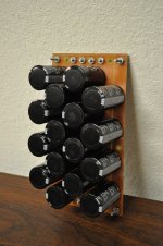
For the heat tunnel, the heatsink is cut in half to create 2 heatsinks 5" x 7" x 2.5". The airflow direction is 7", the heatsink width is 5" and the fin height is 2.5".
Listening results
I have been listening to the amplifiers described above for several days. There are 4 x F5 amplifiers of 2 x F5-balanced amplifiers depending on how you make the input and output connections.
Since one PCB is composed of FQP19N20C/FQP12P20 MOSFETs and the other of FQA28N15/FQA36P15 MOSFETs, listening to the two channels in balanced stereo might be questioned. I did listen to that combo and could not find anything to fault. Likewise, I have been listening to each board as a stereo pair of ordinary (unbalanced) F5s.
Speakers: B&W CDM1
Results:
Balanced: hum and noise absolutely inaudible with ear directly at speaker cone.
Unbalanced: hum and noise barely audible with ear directly at speaker cone.
Listening to a variety of Jazz (Charlie Byrd, Miles Davie, Stan Getz, Scott Hamilton, ...) at "normal" listening levels, I could find no fault with the sound quality, and no perceptible differences between the amplifiers. Maybe someone with better ears could detect a difference, but not me.
Small footprint F5-Turbo
I have modified my V1.1 circult board to support the F5-Turbo diodes.
The modified board will support the following:
1. 1 x Balanced F5
2. 2 x Unbalanced F5
3. 1 x Balanced F5-Turbo-V2 with single MOSFET
4. 2 x Unbalanced F5 Turbo-V2 with single MOSFET
5. 1 x Unbalanced F5 Turbo-V1 with 2 MOSFETs
6. 1 x Unbalanced F5 Turbo-V2 with 2 MOSFETs
- Status
- This old topic is closed. If you want to reopen this topic, contact a moderator using the "Report Post" button.
- Home
- Amplifiers
- Pass Labs
- Balanced F5 in a Small Footprint