main difference with -f5-meets-buzquito:
R14 R16, ( i like this trick!)
exact resistor values to be detrermined
with 2sk2013 2sj313 if I can get them
psu 32 volts plus 5 volts for drivers
and cascodes for jfets
thanks for your help
comments welcomed
cheers
Paul
Hi Paul
Your latest schematics does not really fit in this thread but more in the f5-meets-buzquito thread if it is no more common source output stage. ...
")
here are more thinking:
R7 and R10 to smooth dissipation in M3 and M4 (values to be determined with CISS rise with lower voltage across M3 and M4) advice welcomed
R14 and R16 with CTN to adjust bias independently of gain
R24 and R4 to choose / balance gain of devices
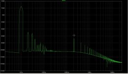
notice high value of R5: 47k! with C2 forms a low pass and seems to give very good results in LTSPICE on square signal 100kHz with C1 (much less noise on fft analysis and no overshot!)
I took M3 M4 IRF9640 IRF530 available in LTSPICE, I read with interrest f5-meets-buzquito and would like to find the best compromise: not obsolete, VGSoff>2volts, low power TO220?... and probably mount them on a small independant dissipator... R1 and R9 could be 100 ohm or more in a linear region.
as for OLG / NFB ... and linearity I am a newbee I do not know where to go!
and SPICE is not real life, shure we are all aiming for the best, that's the magic of this site!
cheers
Paul
Hi Paul
R7 and R10 just limits the possible voltage swing of the stage. Just use a proper dissipator instead...
Your input low pass filter is for 15392 Hz

The p-mosfet I indicate in the first post schematics are readily available and have a VGSoff of 3 to 5V (TO-220) which is what is required. The IRF device are not the best device for linearity...
For R1 and R9 you want a medium current to drive the output mosfet and operate in the more linear current portion of the medium power mosfet transistor... so you should stay with a lower value than 100 ohms... Again, see the first post schematics.
For the OLG/NFB, my goal is to obtain a similar one as the original F5 thus the schematics of first post...
Thanks
Fab
and the winner of the day is....
Thank you Fab for your interrest and support
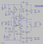
this one will remind you something!
seems to work very well on square signals: no overshot with 1uF on output,
real JFET would be : 2N5462/5459, unless you suggest differently...
OLG: about 48dB /1pair/8Ohm , will need two pairs of laterals for bass channel (4Ohm)
not too sure about temperature compensation, main concern is with input jfets
the bias jfet:2.4 mA/1...4 volts so less heat than inputs, reduce cascode voltage...
or elaborate some sort of compensation or automatic bias, thermistor will not help much IMO.
cheers
Paul
Thank you Fab for your interrest and support
this one will remind you something!
seems to work very well on square signals: no overshot with 1uF on output,
real JFET would be : 2N5462/5459, unless you suggest differently...
OLG: about 48dB /1pair/8Ohm , will need two pairs of laterals for bass channel (4Ohm)
not too sure about temperature compensation, main concern is with input jfets
the bias jfet:2.4 mA/1...4 volts so less heat than inputs, reduce cascode voltage...
or elaborate some sort of compensation or automatic bias, thermistor will not help much IMO.
cheers
Paul
Attachments
A question or three:
I see the cascode resistors R10 & 18 tied to Signal Ground.
Q1.) would the circuit still operate properly if these two resistors were detached from Ground and just connected to each other?
Or
Q2.) do each of the cascodes need to be referenced to a ground to operate properly?
Q3.) would performance deteriorate if these resistors were tied into Power Ground?
Last edited:
hello andrew
I did not intend to design anything special for R10 18, just rushing the drawing...
Q1 I would say yes, some people do it, I think use one 10k res and one cap for same result, but please take advice from other people as well!
Q2 IMO: no
Q3 as long as you use a good decoupling cap, i should work ok
... I'm no professionnal, other people will certainly be more competent
Paul
BA-3?
I expect you have found it by now
btw, it was our good man Juma with the thread 'F5 meets Buzquito'
now that I think about it, he might have inspired Nelson to design the new F5 like frontend/driver for the BA3

did you think of BA-3 with laterals instead of F5 ?
guess Im as good as dead now
I expect you have found it by now
btw, it was our good man Juma with the thread 'F5 meets Buzquito'
now that I think about it, he might have inspired Nelson to design the new F5 like frontend/driver for the BA3
let's just say that some things are boiled water for Curl , Borbely and Pass .
in whatever line-up you line them
Sorry, but that way you'll make a popular mistake known as "starved JFETs" which is manifested through grainy & murky sound. To correct it, go for JFET's Id = 70-90% of Idss.... the bias jfet:2.4 mA...
thanks Juma, I am on the learning curve, reading lots of threads here and playing with LTspice, hoping that simulation is not too far from real life, I know that I will have to experiment, maybe audiotester (another unknown tool) will tell me if I am right,
I have an old scope too, but dead signal generator....
I think I will opt for a VAS circuit, with BJT(15mA bias),
Laterals, double die 150...500mA bias
looks more stable, less concern with thermal compensation
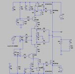
Thanks to all here, the following schematic owes to you too Juma
Paul
(and sorry if I should not post in Pass Lab)
I have an old scope too, but dead signal generator....
I think I will opt for a VAS circuit, with BJT(15mA bias),
Laterals, double die 150...500mA bias
looks more stable, less concern with thermal compensation
Thanks to all here, the following schematic owes to you too Juma
Paul
(and sorry if I should not post in Pass Lab)
Attachments
Sorry, but that way you'll make a popular mistake known as "starved JFETs" which is manifested through grainy & murky sound. To correct it, go for JFET's Id = 70-90% of Idss.
If you look closely at his schematics of post #23, the source resistors are 10 ohms which is clearly within the 80-90% Idss range. The 2.4ma that he indicates may be simply its spice model of Idss of 3ma or so.
However, in Paul post #33 he made the mistake with 22 ohms as source resistors..
Maybe it gives about 50-60% Idss or so thus is it so bad?
Last edited:
thanks Juma, I am on the learning curve, reading lots of threads here and playing with LTspice, hoping that simulation is not too far from real life, I know that I will have to experiment, maybe audiotester (another unknown tool) will tell me if I am right,
I have an old scope too, but dead signal generator....
I think I will opt for a VAS circuit, with BJT(15mA bias),
Laterals, double die 150...500mA bias
looks more stable, less concern with thermal compensation
Thanks to all here, the following schematic owes to you too Juma
Paul
(and sorry if I should not post in Pass Lab)
Hi Paul
The bias of the output mosfet is depending on the VAS current in this type of configuration thus voltage across your 120 ohm resistors. Depending on your LAteral mosfet VGSoff, the VAS may have to be quite different than 15ma. In order to keep at least the 15ma, you may have to change the 120 ohm value.
And for the VAS transistors, the ones you have selected are quite good for this job. However, if you compare with a mosfet VAS you will find a drastic change in the sound (more "alive", if I try to describe it...) although the electrical performance is worse than with good BJT in VAS (as you indicate also more stable in temperature). Some may like it more with good mosfet VAS (like me) or not. It is a matter of taste here..
Fab
Last edited:
I think that current through input JFETs in that sch. is determined by J3 and J4 (they both act as constant current sources).If you look closely at his schematics of post #23, the source resistors are 10 ohms which is clearly within the 80-90% Idss range. The 2.4ma that he indicates may be simply its spice model of Idss of 3ma or so.
I think that current through input JFETs in that sch. is determined by J3 and J4 (they both act as constant current sources).
My mistake Juma, of course you are right.
- Status
- This old topic is closed. If you want to reopen this topic, contact a moderator using the "Report Post" button.
- Home
- Amplifiers
- Pass Labs
- F5 Semi-Turbo with Lateral Mosfets...