4.4mA front end bias, in itself, is fine.
But since I expect you to get more bias current then Dave (who has the right value compared to theory), something is NOT right with your current PCB.
I have no idea what you have on your PCB and what not, it is impossible for me, or anyone, to do remote debugging for you.
For example if your outputs are connected to Gnd then the 55R feedback resistors are in parallel with the 11R, and your degen is then not 11R, but more like 9R1.
You have enough JFETs, so you can first test a JFET of roughly the same Idss offline and convince yourself what Id you should get with 11R degen.
And then you should go back to your PCB and find out if there are any discrepancies.
Have a go first.
Patrick
I'm still trying to troubleshoot this one......
I think it has something to do with the "grounded X" configuration that is recommended while setting up. When the "grounded X" jumpers are in (see post #9), the JFETs are biased differently as the outputs are grounded by the 220R resistor (R21/22) in this configuration.
Maybe Dave's JFET bias measurements were done in the "floating X" configuration

No. Grounded X is fine for testing, as in 2x single ended.
The output resistors to ground will make little difference, as you essentially has a source resistor of 11R // (55R + 220R).
If anything the current should be more rather than less, since less degeneration.
As I said, satisfy yourself on a breadboard what current you should get with the degeneration resistor values.
Measure those values on the PCB to make sure they are as should be.
Trace to see where the current is "gone".
You can also verify the actual current by either the drain resistors (make sure you measure their values first before applying voltage).
Or use an ammeter.
Patrick
Connections
I have a few questions :
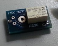
1) The BOM for the 'Mute' board states that there is one BAW 76 diode. Where do I solder this on? Please refer image 'Mute'.
2) For the input board connection to the main board, I will need to solder the joints as indicated in image 'input connection'. Are these connections correct?
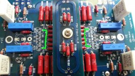
3) As for the jumpers between Q7A and Q10A and Q11A and 14A, again please refer to the image 'jumper', is this correct?
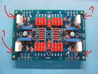
4) What are the uses of these holes on the boards? Please refer to image 'holes'. I have soldered the source resistor without elevating them and so I was thinking of drilling a parallel holes beside these. Then I will connect a wire under the board from these holes to the source resistors so I would take measurement from there. if not, what other possible way to measure these resistors?
Thanks
PM Choong
I have a few questions :
1) The BOM for the 'Mute' board states that there is one BAW 76 diode. Where do I solder this on? Please refer image 'Mute'.
2) For the input board connection to the main board, I will need to solder the joints as indicated in image 'input connection'. Are these connections correct?
3) As for the jumpers between Q7A and Q10A and Q11A and 14A, again please refer to the image 'jumper', is this correct?
4) What are the uses of these holes on the boards? Please refer to image 'holes'. I have soldered the source resistor without elevating them and so I was thinking of drilling a parallel holes beside these. Then I will connect a wire under the board from these holes to the source resistors so I would take measurement from there. if not, what other possible way to measure these resistors?
Thanks
PM Choong
Attachments
Last edited:
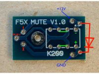
1) BAW76 goes to the RHS of the relay as in your photo. The cathode should face the positive side of the relay (i.e. diode normally off).
2) Yes, except that there are only 6 connections between the two boards. The one next to R10 is not connected to the main board.
3) Not correct. Please refer to Dave's instructions and schematics again. You can also see from your "holes" photo which 2 holes per Q7B and Q10B and Q11B and 14B have solder.
4) They are spare holes which have no use for you. You need to lift the power resistors off the PCB (at least 2~3mm), else your PCB will not last very long.
Hope this helps,
Patrick
> BAW76 goes to the RHS of the relay as in your photo. The cathode should face the positive side of the relay (i.e. diode normally off).
What is the RHS?
> 2) Yes, except that there are only 6 connections between the two boards. The one next to R10 is not connected to the main board.
Do you mean the one connected to R101 on the input board? What is this hole for
Thanks!
Nic
What is the RHS?
> 2) Yes, except that there are only 6 connections between the two boards. The one next to R10 is not connected to the main board.
Do you mean the one connected to R101 on the input board? What is this hole for
Thanks!
Nic
Hi Nic, Patrick,
Dave
Measured groundedX for the build article. Still had one of both configs available to test though so - Measures esentially the same either way. The current has to be going somewhere else as Patrick suggests or there is something wrong. Can you take at least one complementary pair of the JFETs out and do the simple Idss testing with an 11R resistor at 16V?Maybe Dave's JFET bias measurements were done in the "floating X" configuration
Right Hand SideWhat is the RHS?
That wire goes up to the mute relay board, not down to the main amplifier board.Do you mean the one connected to R101 on the input board? What is this hole for
Dave
Yesterday evening I build a test-circuit to do these measurements (and others) and I have now collected data.Can you take at least one complementary pair of the JFETs out and do the simple Idss testing with an 11R resistor at 16V?
In fact, I think I have found at least part of the explanation. The Idss values measured using the tracer (locky_z) are about 1 mA higher than what I measure with a "classical" method using the circuit you/Patrick presented in one of the first posts and a good DMM.
The difference is in terms of absolute values, not in term of relative values, and considering the 1000 FETs I have measured and matched using the tracer data (+ in silico calculations) I am very happy to see it all fits very nicely.
Anyway, back to the amp:
The Idss of a similar FET without degeneration is 6.7 mA (7.9 according to tracer). After 11R degeneration the (measured) value is 5.2 mA. Better, but still about 0.5V off what I measure in the amp.
The current over the drain resistor(s) is about 10.2 mA, leaving me even more perplexed.........
Thanks.
Please see attached images.
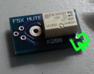
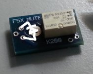
1)Which side is the RHS? Is image 'Mute 1' or 'Mute 2'?
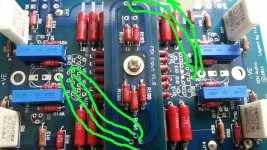
2)Please refer to image 'connection to Mute'. Is this connection correct? Do the other holes connect to the Mute board as well as indicated by the dotted lines?
3) i have raised the source resistor about 4-5mm above the board.
Thanks again.
PM Choong
Please see attached images.
1)Which side is the RHS? Is image 'Mute 1' or 'Mute 2'?
2)Please refer to image 'connection to Mute'. Is this connection correct? Do the other holes connect to the Mute board as well as indicated by the dotted lines?
3) i have raised the source resistor about 4-5mm above the board.
Thanks again.
PM Choong
Attachments
1) None of the above. The diode is soldered electrically in parallel with the relay coil with the cathode to the positive side of the relay coil.
Please kindly read the datasheet of the relay to find out which pins are for the coil, and which is positive.
2) The connection to the Mute board is correct. 4 connections altogether. I do not have these boards, as they are Dave's layout. So he should confirm.
There is also one green line missing going from the input board to the RHS of your picture.
So 6 connections altogether between main & input board.
Dave please cross check.
Patrick
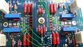
Mute PCB
My (limited) understanding:
Connections to input PCB in red.
Relay data sheet indications in green.
Connections to control board in blue.
When the relay is unpowered (green lines) the amp inputs (1, 2) are grounded via a 10R resistor (R101) on the input PCB.
My (limited) understanding:
Connections to input PCB in red.
Relay data sheet indications in green.
Connections to control board in blue.
When the relay is unpowered (green lines) the amp inputs (1, 2) are grounded via a 10R resistor (R101) on the input PCB.
Attachments
Ok. Removed the bipolar transistors, but also R13 and family.
The current draw from the supply lines now quantitatively corresponds to the predicted current draw from the degenerated transistors (measured on very similar Idss/Yfs transistors not in the amp).
I however still cannot make current over the 11R resistor fit exactly.
While measuring I realized that I can calculate Yfs, without the tracer measurements, as long as I have Id measurements with two different values of degeneration (for example 0R and 11R).
The relationship is the following:
Yfs = (Id(Rdeg1)/Id(Rdeg2) - 1)/(Rdeg2-Rdeg1)
Could be useful if one would like to transconductance match transistors with a simple DMM.
Cheers,
Nic
Shorting out the Q9 11R resistor(s) increases current by 1.74 mA, which is similar to what I predict from FET measurement (6.79 - 5.15 (11Rdeg) = 1.64 mA). I think this is close enough and conclude that most likely everything is 0k.
Next question:
Dave suggests to start with a start bias of 1.5A and I know both Vgs and Yfs @2A for my MOSFET's. Therefore I guess I can estimate my start Vgs by the following relationship:
Vgs@1.5A = Vgs@2A - (2A-1.5A)/Yfs@2A
I know I will be underestimating as the curve is not a straight line, but anyway
In my case the result is just 63 mV lower than Vgs@2A so maybe a thump rule of 0.1-0.2V below Vgs@2A is safer.
Last question:
any recommendations for bolting down the MOSFET's? I must admit that this is my first class A amp build, where thermal conduction obviously is critical.
How much "muscle" should I put into the tightening?
Should I use washers/bars to distribute the pressure on the FET?
Re-tightening when warm?
Cheers,
Nic
> Vgs@1.5A = Vgs@2A - (2A-1.5A)/Yfs@2A
Close enough as first approximation.
But have you not forgotten about the voltage across Rsource ?
> In my case the result is just 63 mV lower than Vgs@2A
Really ?
Your FETs have 8 Siemens transconductance at 2A ?
You have them all curve traced, So why not look up the actual Vgs at 1.5A
> any recommendations for bolting down the MOSFET's?
Single M3 is provided on the heat sink.
Use stainless steel (non-magnetic) cap head screws with Torx or Allen key (hex) drives.
Use spring washer plus plain washer between screw head and MOSFET.
Tightening torque ~0.5Nm (the tapped hole is AL and not steel).
> Re-tightening when warm?
In theory the spring washer will compensate for any thermal expansion.
You are not using any grease or phase-change thermal compound.
So I don't bother myself.
But check it to convince yourself, by all means.
Patrick
>Really ?
Your FETs have 8 Siemens transconductance at 2A ?
You have them all curve traced, So why not look up the actual Vgs at 1.5A
Calculation error. The number is 0.125V (=(2.0-1.5)/4)). The GB mosfets have Yfs@2A in the 3.5 - 4.5 Siemens range.
Of course I can look up the measured value for Vgs@1.5A. And of course I can do this for all the GB members........
Interested members can PM me their FET numbers (one will be sufficient as they are matched devices).
Thank you for the useful info on bolting down the FETs. Maybe the bolts are included in the chassis kit.
Cheers,
Nic
- Home
- Amplifiers
- Pass Labs
- F5X -- the EUVL Approach - The Build Thread