
Input bias is fixed by the Idss of the JFETs (and the resistor network.
We supplied them to the GBs, so they will not be 8mA.
We know.")
You can actually do a first test without the MOSFETs.
By applying power and measuring the voltage across the drain resistors, you know the Vgs bias value.
And since you know how to match MOSFETs from the UDNeSS project, you can also measure the Vgs at 2A.
Then you can compare the two values, while adding the additional voltage across the 0R22 source resistors.
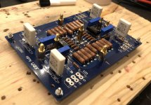
The board looks real nice.
Patrick
We supplied them to the GBs, so they will not be 8mA.
We know.
You can actually do a first test without the MOSFETs.
By applying power and measuring the voltage across the drain resistors, you know the Vgs bias value.
And since you know how to match MOSFETs from the UDNeSS project, you can also measure the Vgs at 2A.
Then you can compare the two values, while adding the additional voltage across the 0R22 source resistors.
The board looks real nice.
Patrick
See P.15 of Nelson's article.
http://www.firstwatt.com/pdf/art_f5_turbo.pdf
I'll see if I can find a picture of my own boards.
P.
http://www.firstwatt.com/pdf/art_f5_turbo.pdf
I'll see if I can find a picture of my own boards.
P.
I cannot find a picture, but this is how I connect mine.
The red wires do not touch the middle star Gnd.
Best to use enamel wires or teflon insulated copper/silver wires (single strand).
You can of course use an X, solder in the middle, hanging above the Gnd terminal connection, for a true F5X.
Electrically the same. Optically not.
Patrick
.
The red wires do not touch the middle star Gnd.
Best to use enamel wires or teflon insulated copper/silver wires (single strand).
You can of course use an X, solder in the middle, hanging above the Gnd terminal connection, for a true F5X.
Electrically the same. Optically not.
Patrick
.
Attachments
Some more progress from today. I have set the Vgs value now to 2V without the MOSFETs but I have not measured their Vgs @2A. I’m a bit hesitant to do measurements with the Xen super-matched unobtainium parts so that I wouldn’t break them while measuring.
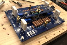
I was planning to use my current UDNeSS case heatsinks to test my F5X with MOSFETs and bias currents. According to CeeVee the drill pattern is the same as diyAudio UMS. Of course that is a risk too to make some damage...
I was planning to use my current UDNeSS case heatsinks to test my F5X with MOSFETs and bias currents. According to CeeVee the drill pattern is the same as diyAudio UMS. Of course that is a risk too to make some damage...
Attachments
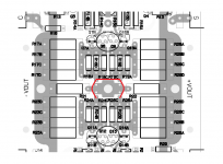
MOSFET mounting holes are 120mm (across) x 80mm
The Vgs of the MOSFETs at 2A bias 65°C is about 2.3V.
Add 0.44V across the MPC74's, you will need 2.75V to get to final bias.
At 2V, you might not get any current at all.
I would at least start with 2.3V.
The PCB is proven. Many examples built.
And you can always set the current limit at your lab supply to say 1.5A to be safe.
And then increase gradually.
Patrick
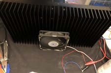
So I decided to go forth and tested my F5X with power MOSFETs in place. I used the sinks from my UDNeSS/M2x chassis equipped with a cooling fan and I powered the thing with my lab supply.
I had adjusted the Vgs voltage to 2,25 V without the MOSFETs and it gave me a comfortable starting point with 1,05 A bias. Then I slowly adjusted the pots and the bias was easily settled to 2 A. Even the DC offset was only about 8 mV without further adjusting. After one hour the sinks were about 38 C and the highest reading I got from the MOSFETs was ~56 C. The fan really makes a big difference and without it these sinks would be inadequate.
Now I can be sure that I haven’t made any silly mistakes and can continue with soldering the other channel while waiting for the enclosures.
Attachments
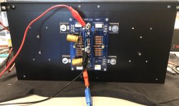
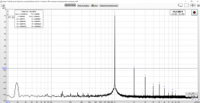
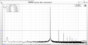
Some distortion measurements with +-16V rails from lab supply, 2 A bias and 1 W into 8 ohm load. These were with REW internal signal source, I will test with VicNic osc when the amp is complete. Measurements were done for +out and -out separately with grounded X connection.
Everything seems to be in order. The -out half has little less distortion but profile is very similar.
Everything seems to be in order. The -out half has little less distortion but profile is very similar.
Attachments
- Home
- Amplifiers
- Pass Labs
- F5X -- the EUVL Approach - The Build Thread