Regarding heatsinking how do I calculate the Tj for multiple transistors on the same sink?
Single transistor: Tj= 25+(32x(0.83+0.1+0.28) where 0.1 is the keratherm pad and 0.28 is a big 200x200x40 heatsink. Tj=63.72C
now if I double the power dissipation I get:
Tj= 25+(64x1.21)=102.44 but this formula doesn't account for 2devices, just 1 dissipating double the power. How do I introduce the 2nd transistor In the formula?
the first term 25 is Ta, is that a reasonable ambient temperature to use?
the second term 32 is the device dissipation.
You must put in there the actual device dissipation.
you must split the last three terms.
0.83 is the device Rth j-c, use this for each single device.
0.1 is the Rth c-s, use this for each single device.
0.28 is the Rth s-a this must be de-rated to take account of the lower deltaT, use this after de-rating for all devices on the sink.
back to Ta.
In Scotland I would use 28degC since I don't have air conditioning.
What would you use for summer Ta?
Last edited:
I understand the formula when used for a single device. what I can't figure is how to write the formula for 2 or 4 devices on the same sink.
Example:
f5t with 4 devices on a sink with 0.20w/c with 1Abias @32v how would I lay the formula?
Ps: Summer Ta would be 30c worst case I think. Must measure next summer")
Example:
f5t with 4 devices on a sink with 0.20w/c with 1Abias @32v how would I lay the formula?
Ps: Summer Ta would be 30c worst case I think. Must measure next summer
Ta=30
Ts= Pdtotal * Rth s-a * DF.
try two dives @ 25W each & Rth s-a = 0.28C/W measured @ deltaT=75Cdegrees.
Ts= 30 + [2*50*0.28*DF] = 30 + 28Cdegrees. 28 is <<75 so DF >>1.00
manufacturers data may say use Df=1.3
Ts= 30+28*1.3 = 66degC
Tc= 25 * 0.1 +66 = 68.5degC
Tj= 25*0.83 +68.5 = 89degC
Tc is needed to calculate the temperature de-rated SOAR.
Need biasing help
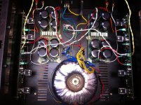
I am about to bias up my F5T v2. I have separate heatsink for each of the MUR3020W diodes near the output devices.
Since I am fraidy cat as Papa puts it, I can start by biasing upto 0.3v on 1 ohm resistor to begin with. My speaker load is nominal 8 ohms and is not going to go very low at all. My question is where do I go after that. My heatsinks are pretty huge and actually meant for v3 and I expect them to run only warm and not hot.
Is there a way to push the bias further than 0.3V ? I want to run as much as possible in Class A mode.
Thanks.
The factor that determines the maximum current you can bias you r output to is the Vdrop across the Rs and heat. If you can deal with the heat, you simply need to change the Rs value to whatever will give you your desired bias, while dropping no more than 3-400mV, like in the article. Example. 2A bias would need .15R resistor to give you a safe V drop for the diodes.
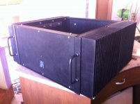
Completed F5T v2 - few problems
Completed building F5T v2 exactly as per the schematic using boards designed by fellow member Om Mishra as a part of a group buy on an India forum.
Heatsinks are massive 20 KGs per meter heavy duty ones.
Pictures are enclosed.
The amp biases nicely and have biased to 350 mv on each channel. Provided individual heatsinks to each of the switching diodes at the outputs. Gets to around 40-45 degrees centigrade. Tried playing music. One channel plays really well and on the other channel there seems to be no gain, with very feeble output. Every resistor is measured and soldered. There cannot be too many errors on the solder as I have gone through each solder with a magnifying lens before powering on.
The power supply is showing 33.5 on each rail on load condition. Could it be the case of a bad jFet pair on the bad channel? Don't know where to look.
Need help from the gang please....
Cheers.
Attachments
make a break for few days
after that , go back and compare channels visually
then power up and compare them with DMM
Thanks. I think you are right. Having spent two full days on putting it together, I definitely need some rest.
Bad jfet is easy. Test V drop across source resistors. Take voltage readings at various places, starting with FE. Report back. All this after taking a break, as ZM suggested. It is amazing how many mistakes I have found after taking some time away from a project.
Yes, I have a good identical channel to compare the readings. One more thing the jFets are at 8.7 mA IDSS and the supply voltage is 33.5 V DC per rail. Papa's article talks of 8 mA IDSS. I dread desoldering on a thick doubled sided PTH PCB.
Thanks.
Is that Idss measured in circuit or before installation. Are both channels showing that Idss? That seems high for a degenerted BL grade. IT is possibly too high in terms of dissipation, but ZM may have more insight in this particular area.
IDSS rating given by spencer and is measured before the installation.
Nice case, Anil
Bad input FET is what it might be. There was someone who had the exact same problem on the F5 thread and there were some questions on being able to set the bias with a busted jFET, but apparently it is possible.
I wouldn't worry about desoldering from a double sided board. Just snip off the leads and solder the new transistor on top of the pad (no need to go all the way through). Works when the holes won't open up. Mostly though, a hot iron (very hot) an bit of solder to get the flow going, and some solder wick does the job of opening up great for me. Never had an issue even with very tiny through hole components.
Good Luck, the amp looks nice!
Thanks Sangram. How is your Turbo build coming along. I saw the pictures of your cabinet.Nice case, Anil
Bad input FET is what it might be. There was someone who had the exact same problem on the F5 thread and there were some questions on being able to set the bias with a busted jFET, but apparently it is possible.
I wouldn't worry about desoldering from a double sided board. Just snip off the leads and solder the new transistor on top of the pad (no need to go all the way through). Works when the holes won't open up. Mostly though, a hot iron (very hot) an bit of solder to get the flow going, and some solder wick does the job of opening up great for me. Never had an issue even with very tiny through hole components.
Good Luck, the amp looks nice!
First I will measure and compare the working and the problematic boards before I change any component. Surprisingly the amp biases very well.
Cheers.
- Home
- Amplifiers
- Pass Labs
- F5 Turbo Builders Thread