F5T biasing
As you did not give a specific recommendation I chose to increase R5/R6 which to me is just an extension of the range of resistance of P1/P2. The immediate result was the massacering of a set of MOSFETs illuminated by some bengal fireworks in my chassis box. Simple reason was
a) not having zeroed P1/P2 before pushing ON button
b) having chosen 5k in series with R5/R6
Now I know, that my PSU is powerful enough to blow and burn 2 pairs of IRFP240/9240 within sec's.
With the other channel left still in proper condition I tried more carefully adding 330Ohms only in series with the 1k pot and certainly turned it to zero. Now I got exactly what I expected: I was able to tune easily to Iq=800mA/device and still had some turns left, so I am sure I can go to 1A and probably beyound. As you mentioned, that the bias of the JFETs could be affected I measured voltage across R7/R8 but it did not move at all.
Question: Are there any objections against this change from R5=1k to R5=1.3k???? Doesn't sound dangerous to me.
F5T biasing
Hello Andrew,
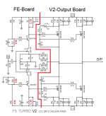
I am fighting the mechanics of this Forum. Tried to embed into the text as others did but seems not to work. I have added it as an Attachement and wonder how this works. Wuill see. I have marked all components in red which I have changed from the original. Everything else is just like the schematic (guess this is what you call "sch") in the build guide of 6L6.
Hello Andrew,
I am fighting the mechanics of this Forum. Tried to embed into the text as others did but seems not to work. I have added it as an Attachement and wonder how this works. Wuill see. I have marked all components in red which I have changed from the original. Everything else is just like the schematic (guess this is what you call "sch") in the build guide of 6L6.
Attachments
Using too much resistance in parallel with the pot will:
a) make the adjustment too sensitive
b) leave room at the top of the adjustment that allows toasting outputs
You've already discovered (b). But as long as you zero the pot before each run, and monitor the output temps, you can prevent toast even with a really big R5/R6.
So if you are fearless (ie: you believe you'll always re-zero and will always watch your temps when adjusting the bias), then any value of R5/R6 that doesn't make the adjustment too sensitive is fine.
If you worry about (b), then step R5/R6 up slowly until you've got just a little bit of room on the pot above where you want to be. It sounds like you're already there if you want 800mA (and possibly even 1A). If you do run out of room again, you may need to go up a bit higher.
Cheers,
Jeff.
F5T biasing
Thanks Jeff, for very usefull comment!
I will stay for a while with the 800mA as my heat sinks are too small anyway. After adding some fins I hope I can go to 1A or more pending on the temp rise. Then I will do exactly what you said, adding resistance to R5/R6 just enough to get the desired Iq plus 1 turn left for final trim.
You have done the correct modification to get adequate bias voltage to suit the output devices you have.
I suspect your jFETs have slightly lower Idss than the average Builders.
6L6,
It seems this problem of inadequate bias voltage crops up occasionally.
I wonder if the Build Guide needs some rewording/explanation on what procedure to follow when bias turns out to be too low?
How about incorporating a table of values of Idss vs R5/6 values?
F5T biasing
Yes, you are right, Idss is low and measured across R3/R4 it is about 4.5mA. Per NP's article this should be 8mA, shouldn't it? Do I need to do something about it?
How do I get it up?
I do use cascoding because of rail voltage of 40V idle. I noticed however, that voltage drops to about 35V when biasing one channel only with 800mA. Guess it will drop further, when I add 2nd channel as well and maybe even go to 1A bias. If it approaches 33V or so, should I swap cascoding at all or is that too "fearless"?
It probably would help overall gain which is a bit low anyway, not allowing to drive the F5T directly from a signal source without preamp.
I have a BA3 gain stage board in my inventory which I may add for more gain. Anybody having done this as well?
F5T biasing
Jeff, I wasn't sure if your comment about the "ZV9 article" was adressed to Andrew or myself. I looked at that article and sure it's always delighting reading NP's papers. However, as this is a very much different device and not really relating Vgs to Idss it will not quickly help me deciding if and how I need to tweak Idss of the 2SK170/2SJ74.
Do I have to do something about the Idss=4.5mA?
Idss=4.5mA means you have used a GR rated 2sk170.
The spec requires a BL rated device.
But you can still get the necessary drive voltage to the output devices by altering the drain load resistances.
Earlier you stated
Measuring the voltage drop across the source resistor allows one to determine the Id, i.e. the actual quiescent operating current. This is NOT Idss.
The spec requires a BL rated device.
But you can still get the necessary drive voltage to the output devices by altering the drain load resistances.
Earlier you stated
you cannot measure Idss in circuit.Idss is low and measured across R3/R4 it is about 4.5mA
Measuring the voltage drop across the source resistor allows one to determine the Id, i.e. the actual quiescent operating current. This is NOT Idss.
Jeff, I wasn't sure if your comment about the "ZV9 article" was adressed to Andrew or myself. I looked at that article and sure it's always delighting reading NP's papers. However, as this is a very much different device and not really relating Vgs to Idss it will not quickly help me deciding if and how I need to tweak Idss of the 2SK170/2SJ74.
Yeah, that was just in support of Andrew's idea of having a table/graph. I won't help you with the F5T.
Do I have to do something about the Idss=4.5mA?
As Andrew stated, what you measured is Id rather than Idss. (Idss will be higher.)
In any case, the only thing you would need to do with a lower Idss is to raise the drain resistors to allow reaching the desired bias point (which you've already done).
Cheers,
Jeff.
When I built my F5V3 I had jfets that biased up at just less than 6ma. I had trouble getting to 250mv bias. I increased the series resistor to 1.5k and zeroed the pots to make sure there wouldn’t be any exploding mosfets. It is a bit time consuming to have to do the biasing over again. It may be useful to provide some general advice in the build guide for when you can’t reach your target bias point.
F5T biasing
Andrew, I bought a set of devices from the DIY store assuming they know which grade and brand. I was checking the data sheet of Toshiba and the BL-grade is rated at Idss=3mA there.
Refer to data sheet attached.
To Bfpca: Yes, I went exactly through this same biasing procedure and ended up with R5/R6 being 1.3k which gives sufficient bias for the Output stage.
By now we are discussing the bias of the JFETs which is said to be 8mA in NP's F5T article but my reading is 4.5mA only. Did you find a way increasing Idss of the JFET's???
Attachments
F5T biasing
First I apologize for not having read the data sheet carefully. Looking at the graphs of page 2 of the Tosh data sheet I do see, that indeed this is different from Id which is what I measured across the 10Ohm resistor.
Thanks for teaching me my celtic friends.
If I understand Jeff correctly, the advice of increasing drain load was already done by changing R5/R6 to 1.3k, right??
Per the description on the DIY store page, they are selling the B-grade of the LSK170 which is equivalent to the BL-grade of the Tosh device. So the device probably is OK and doesn't need replacement.
As 6L6's build guide was completed in 2014 and never updated (I guess), the chance is, that the community is reinventing the wheel on such common issues regularly.
Yes, increasing the value of the drain load increases the bias voltage applied between gate and source of the output mosFET.
If you start with a lower current jFET, then you need a slightly higher drain resistance/load to generate the necessary bias voltage.
Some vertical mosFETs (eg. 2sk1503/j201) and most Lateral mosFETs require a very low Vgs to turn ON.
This may require the drain load resistances to be lower than a standard F5 build.
If one used the standard F5 resistance values for the Toshiba 2sk1530/j201 output pair, you would find that most of the jFET current passes through the variable resistor. This would not suit long term reliability of the VR.
Last edited:
- Home
- Amplifiers
- Pass Labs
- F5 Turbo Builders Thread